Magnetron and semiconductor equipment

A technology of magnetron and yoke, applied in the field of microelectronics, can solve the problems of deep depth, narrow corrosion area width, reducing target material utilization rate and corrosion area uniformity, etc.

Active Publication Date: 2015-01-14
BEIJING NAURA MICROELECTRONICS EQUIP CO LTD
View PDF3 Cites 0 Cited by
  • Summary
  • Abstract
  • Description
  • Claims
  • Application Information

AI Technical Summary

Problems solved by technology

To sum up, the magnetron adopts the inner magnetic pole piece and the outer magnetic pole piece whose upper surface is plane, and the horizontal component value of the magnetic field intensity in the edge area of ​​the envelope of the generated magnetic field line is small, while the horizontal component value of the magnetic field intensity in the central area is large, so that The target corresponding to the edge area has a smaller corrosion depth and the target corresponding to the central area has a larger corrosion depth, resulting in a narrower width and deeper corrosion area on the target, thereby reducing the utilization rate and Uniformity of etched area on the target

Method used


Image

  • Magnetron and semiconductor equipment
  • Magnetron and semiconductor equipment
  • Magnetron and semiconductor equipment

Examples


Embodiment Construction

[0051] In order to enable those skilled in the art to better understand the technical solution of the present invention, the magnetron and semiconductor device provided by the present invention will be described in detail below with reference to the accompanying drawings.

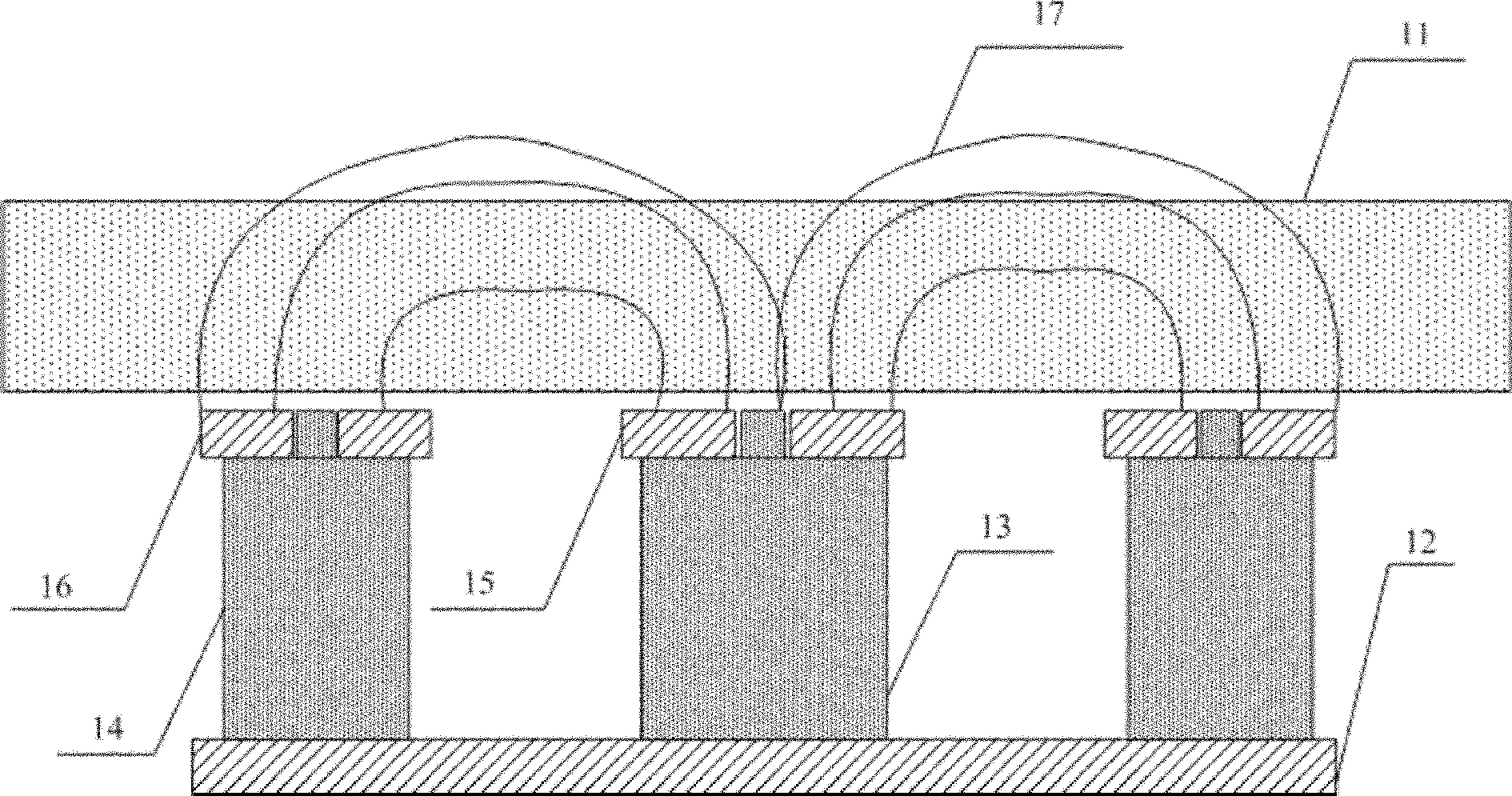
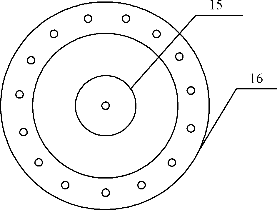
[0052] Figure 5 It is a schematic structural diagram of a magnetron provided in Embodiment 1 of the present invention, Image 6 for Figure 5 Middle A-A sectional view, such as Figure 5 and Image 6 As shown, the magnetron includes: a yoke 21, an inner magnetic pole, an outer magnetic pole, an inner magnetic pole piece 22 and an outer magnetic pole piece 23, the inner magnetic pole and the outer magnetic pole are arranged on the yoke 21, and the outer magnetic pole surrounds the inner magnetic pole , the inner magnetic pole piece 22 is arranged on the inner magnetic pole, the outer magnetic pole piece 23 is arranged on the outer magnetic pole, the magnetic field line emission surface of the inner magne...


PUM


Abstract

The invention discloses a magnetron and semiconductor equipment. The magnetron comprises a magnet yoke, an inner magnetic pole, an outer magnetic pole, an inner magnetic pole element and an outer magnetic pole element, wherein the inner magnetic pole and the outer magnetic pole are arranged above the magnet yoke; the outer magnetic pole surrounds the circumference of the inner magnetic pole; the inner magnetic pole element is arranged above the inner magnetic pole; the outer magnetic pole is arranged above the outer magnetic pole; and a magnetic force line transmission surface of the inner magnetic pole element and a magnetic force line transmission surface of the outer magnetic pole element are slopes respectively. According to the magnetron disclosed by the invention, the magnetic force line transmission surface of the inner magnetic pole element and the magnetic force line transmission surface of the outer magnetic pole element are the slopes respectively and a magnetic field intensity horizontal component value of a magnetic force line enveloped edge area is increased, so that the corrosion depth of a target corresponding to the edge area is increased; the magnetic field intensity horizontal component value of a magnetic force line enveloped central area is reduced, so that the corrosion depth of a target corresponding to the central area is increased, and further, the width of a corrosion area on the target is increased and the depth of the corrosion area is reduced; and in addition, the utilization rate of the target and the uniformity of the corrosion area on the target are improved.

Description

technical field [0001] The invention relates to the technical field of microelectronics, in particular to a magnetron and semiconductor equipment. Background technique [0002] In the manufacturing process of semiconductor integrated circuits, sputtering technology (or physical vapor deposition PVD technology) is used to deposit various metal layers and related material layers. Because copper has the advantages of low resistivity and low electron mobility, the vertical interconnection of metal is generally copper interconnection, in which the metal material is sputter-deposited to a surface with an appropriate aspect ratio. through hole. figure 1 is a partial cross-sectional view of a vertical interconnection structure, such as figure 1 As shown, the vertical interconnection structure includes: a lower dielectric layer 1 , a conductive layer 2 , an upper dielectric layer 3 , a barrier layer 5 and a copper seed layer 6 . The lower dielectric layer 1 includes a conductive l...

Claims


Application Information

Patent Timeline
Patent Type & Authority Patents(China)
IPC IPC(8): H01J25/50H01J23/10H01J37/32
Inventor 耿波李杨超张阳武学伟丁培军
Owner BEIJING NAURA MICROELECTRONICS EQUIP CO LTD
Why Eureka
Try Eureka