EMI shielding in a package module

A technology of electromagnetic interference shielding and packaging modules, which is applied in the direction of magnetic/electric field shielding, circuits, electrical components, etc., can solve the problems of small elasticity and achieve the effect of saving materials

Inactive Publication Date: 2012-07-25
ADL ENG
View PDF3 Cites 19 Cited by
  • Summary
  • Abstract
  • Description
  • Claims
  • Application Information

AI Technical Summary

Problems solved by technology

However, since the shielding range covers the entire package, there is only less flexibility to change the shape and range of the shielding

Method used


Image

  • EMI shielding in a package module
  • EMI shielding in a package module
  • EMI shielding in a package module

Examples


Embodiment Construction

[0028] The present invention will be described in terms of the following embodiments. The descriptions and examples of such embodiments are for illustration only and are not intended to limit the claims of the present invention. Accordingly, the invention may be practiced in substantially equivalent embodiments in addition to those described in the specification.

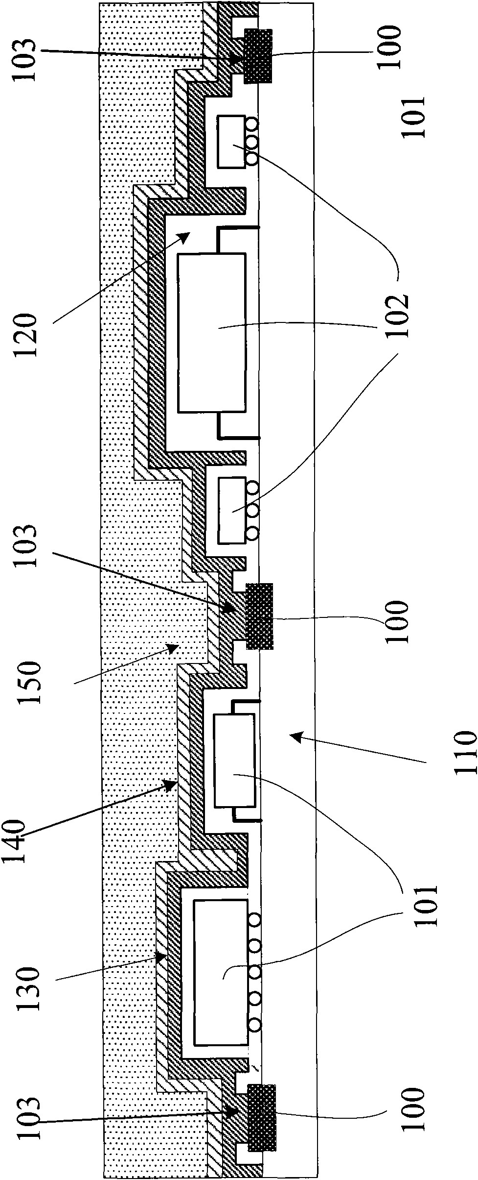
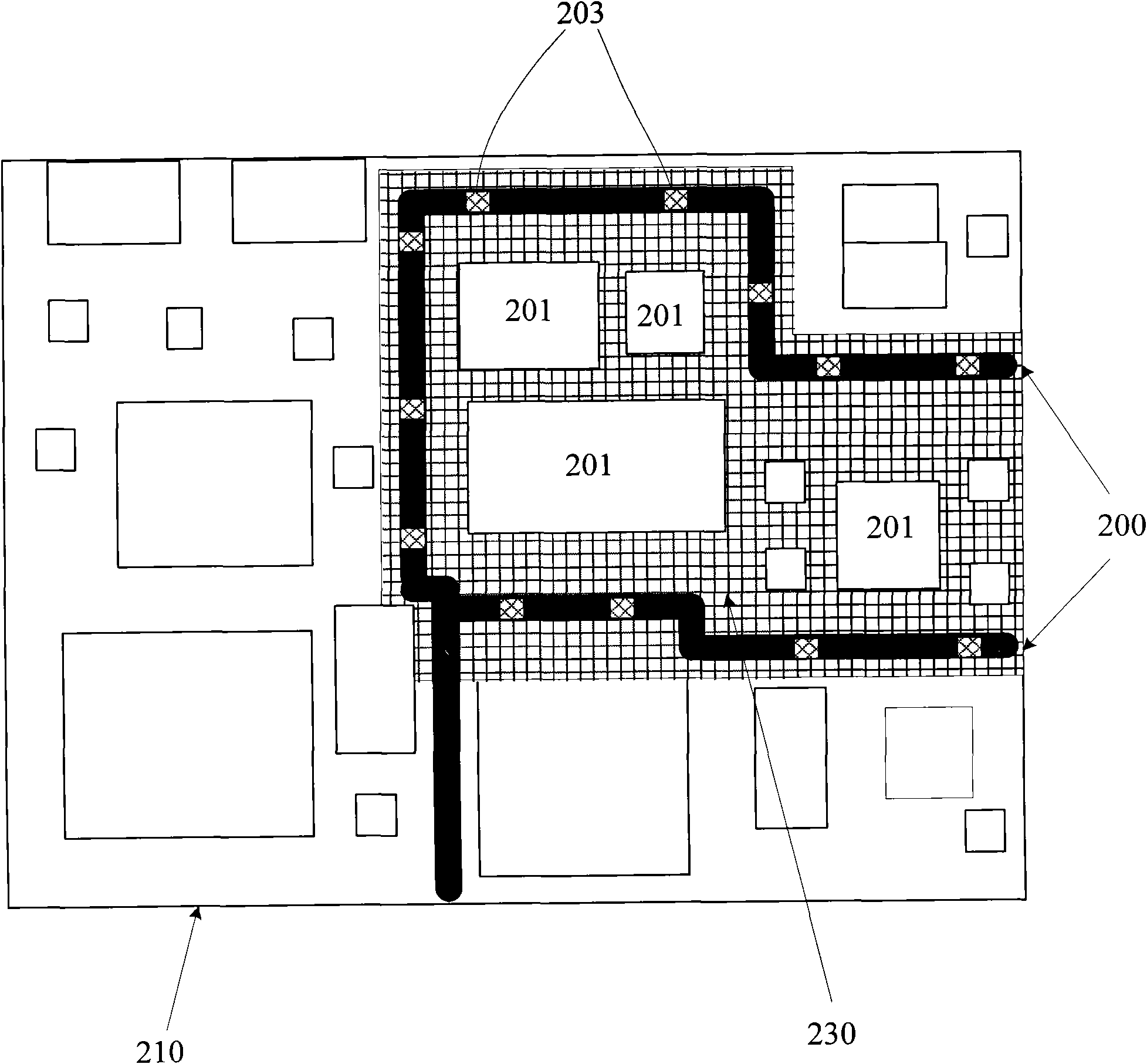
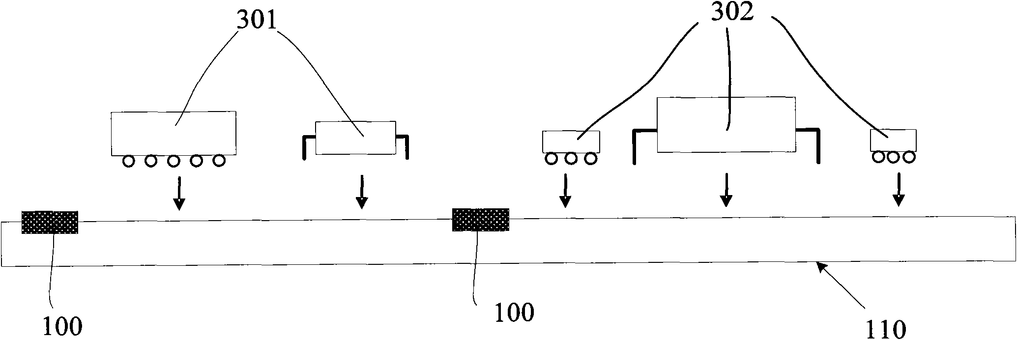
[0029] The encapsulation module with electromagnetic interference shielding and its manufacturing method will be described in detail below. The above encapsulation module has a thin shielding layer. The packaging module of the present invention effectively reduces electromagnetic waves emitted from high-speed electronic devices or electromagnetic waves from other electronic devices. Electromagnetic interference (EMI) between electronic devices or systems will affect the normal operation of electronic products.

[0030] The packaging module of the present invention is not bulky due to the thin shielding layer and ca...


PUM


Abstract

The present invention discloses a package module with EMI shielding and the method thereof. The package module has a substrate or a PCB with at least one ground pad. A variety of electronic components are mounted on the substrate. The dielectric layer overlays a selected area which covers some electronic components and ground pads. Openings are formed within the dielectric layer and above ground pads. The shielding layer with at least two metal layers covers the dielectric layer and is electrically coupled, via the openings, to the ground pad. In general, there is a protection layer to encapsulate the entire substrate. The package module of the present invention not only achieves the requirement of miniature packaging but also reduces EMI caused by high speed electronic devices.

Description

technical field [0001] The present invention relates to electronic packaging modules, and in particular to packaging modules with electromagnetic interference shielding function and miniature packaging characteristics. Background technique [0002] Due to the rapid development of semiconductor technology, the complexity and functionality of electronic products such as mobile phones, televisions, notebook computers, etc. have greatly increased. More and more complex and high-speed semiconductor devices are packaged in substrates or printed circuit boards. High-speed semiconductor devices can generate electromagnetic waves that interfere with other devices, or are interfered by electromagnetic waves emitted by other high-speed devices. Electromagnetic interference (EMI) will negatively affect the operation of electronic systems, and problems caused by electromagnetic interference are common to manufacturers of electronic devices. [0003] One conventional approach to reducin...

Claims


Application Information

Patent Timeline
Patent Type & Authority Applications(China)
IPC IPC(8): H01L23/552H01L21/50H01L21/58H05K9/00
CPCH01L2224/16227H01L2924/19105H01L21/561H01L23/26H01L2924/15788H01L23/552H05K9/0026H01L2224/81191H01L2224/97H01L2924/15787H01L2924/01029H01L2224/16225H01L2924/157H01L23/3135H01L24/10H01L2224/81815H01L24/16H01L24/81H01L2924/181H01L2924/00014H01L2224/81H01L2924/00
Inventor 林南君郑雅云郑靖桦刘广三
Owner ADL ENG
Why Eureka
Try Eureka