Instantaneous harmonic estimation and compensation type single-phase inverter power supply and control method of single-phase inverter power supply
A technology of single-phase inverter and full-bridge inverter circuit, which is applied in the direction of electrical components, AC power input conversion to DC power output, output power conversion devices, etc.
Inactive Publication Date: 2012-07-25
NORTHEASTERN UNIV
2 Cites 17 Cited by
AI-Extracted Technical Summary
Problems solved by technology
[0004] Aiming at the distortion problem of the load voltage waveform caused by the harmonic current on the filter inductor when the inverter power supply has a nonlinear load (such as a rectifier), the present ...
Method used
CU1, CU2 are the D axis of ideal output voltage and the given signal of Q axis, CV1, CV2 are the D axis of actual output voltage and the reference quantity of Q axis, therefore can set up the double circuit of the voltage ring based on D axis and Q axis control strategy. Introducing independent PI controllers in the double loops of the voltage loop can eliminate the steady-state error. The ideal requirement for steady state is when k→∞, (CU1-CV1)→0, (CU2-CV2(t))→0.
Display circuit as shown in Figure 6, display circuit selection model is the liquid crystal module of OCM4X8C8, and TMS320F2808 chip communicates with liquid crystal module OCM4X8C8 by GPIO module, with the form of menu at all levels, the output voltage of real-time display inverter device, Output current, output power, power factor and other parameters. OCM4X8C 8 is a 128*64 dot matrix liquid crystal display module for Chinese characters and graphics, which can display Chinese characters and graphics, and has 8192 Chinese characters built in. The three control ports RS, RW, and EN of the liqui...
Abstract
The invention relates to an instantaneous harmonic estimation and compensation type single-phase inverter power supply and a control method of the single-phase inverter power supply. The single-phase inverter power supply comprises a full-bridge inverter circuit, a filter circuit, an output voltage sampling circuit, an output current sampling circuit, a sinusoidal pulse width modulation (SPWM) driving signal level converting circuit, an insulated gate bipolar translator (IGBT) driving circuit, a display circuit, a press key circuit, a digital signal processor (DSP), a field programmable gate array (FPGA) and a power supply circuit. The direct current inversion, the sampling of output voltage and output current and the SPWM control signal driving can be stably and accurately realized, meanwhile, the matched use of the DSP and the FPGA is adopted, and a control algorithm can be efficiently and fast realized. The method provided by the invention adopts the base wave control based on a D-Q module for ensuring that the output waveform peak value and the phase position stable precision have good dynamic response; the feed-forward compensation and the feedback compensation are adopted, so that the external noise interference and the total harmonic distortion rate in the output voltage can be effectively reduced, and the waveform of the output voltage is perfectly controlled.
Application Domain
Ac-dc conversion
Technology Topic
Single phaseFull bridge inverter +14
Image
Examples
- Experimental program(1)
Example Embodiment
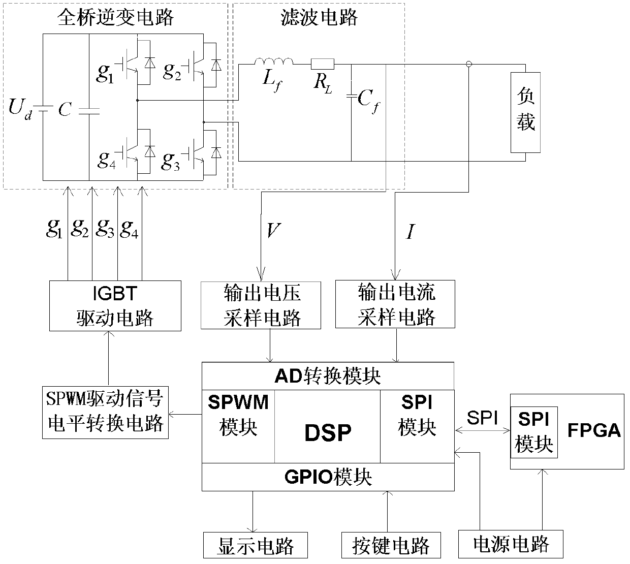
[0112] The specific implementation of the present invention will be further described below in conjunction with the drawings.
[0113] The instantaneous harmonic estimation and compensation type single-phase inverter power supply provided in this embodiment has a power of 3KW, an effective value of output voltage of 220V, and a frequency of 50Hz. The instantaneous harmonic estimation and compensation type single-phase inverter power supply of the present invention, such as figure 1 As shown, including full-bridge inverter circuit, filter circuit, output voltage sampling circuit, output current sampling circuit, SPWM drive signal level conversion circuit, IGBT drive circuit, display circuit, key circuit, DSP, FPGA and power supply circuit.
[0114] The full-bridge inverter circuit includes a DC side filter capacitor and four fully-controlled switching devices IGBT, such as figure 1 As shown, four IGBTg 1 , G 2 , G 3 , G 4 Medium, g 1 And g 4 Form a bridge arm, g 2 And g 3 Form a bridge arm, g 1 And g 3 On and off at the same time, g 2 And g 4 On and off at the same time. The function of the full-bridge inverter circuit is that the four IGBTs transfer the externally input direct current U under the control of SPWM modulation technology. d (For example, direct current from photovoltaic cells, direct current from rectifier, etc.) is inverted into alternating current with a certain frequency or variable frequency to supply the load. The switch device selected in the present invention is the SKM400GB176D module produced by SEMIKRON Company. The module has a maximum withstand voltage of 1700V and a rated current of 400A). The upper and lower bridge arms are encapsulated with two IGBTs and their freewheeling diodes, so the full bridge The inverter circuit requires two SKM400GB176D modules (G1, G2).
[0115] In addition to the expected fundamental voltage, the output voltage of the full-bridge inverter circuit controlled by SPWM modulation technology also contains high-frequency harmonics whose frequency is an integer multiple of the carrier frequency. In order to filter out high-frequency harmonics, the present invention adopts a low-pass filter circuit. The fundamental wave with a lower frequency can pass through the low-pass filter circuit without attenuation in amplitude. The harmonics with higher frequency have amplitude after passing through the low-pass filter circuit. Will be greatly attenuated. Such as figure 1 Shown, L f Is the filter inductance, C f Is the filter capacitor, R L For L f The internal resistance.
[0116] Output voltage sampling circuit such as figure 2 As shown, it includes a transformer, a proportional amplifier circuit, a voltage signal raising circuit, and a limiting circuit. The output voltage sampling circuit is used to convert the output voltage signal of the inverter power supply (the peak value of the fundamental voltage is 311V) into the range of 0V to 2.14V The voltage signal is sent to the AD module of DSP. The DSP model selected in the present invention is TMS320F2808. The chip contains 16 channels of 12-bit AD conversion modules, and one of them is taken to collect AC voltage signals. The output voltage signal of the inverter power supply is connected to the terminal labeled "Inverter Voltage" via a wire. The output voltage signal with a fundamental peak voltage of 311V is passed through a self-made transformer with a transformation ratio of 220:9 and a working frequency range of 50Hz to 600Hz. Converted into an AC voltage with a peak value of 12.73V, and then divided by the voltage divider resistors R1 and R2 to output an AC signal with a peak value of 6.36V. The 6.36V AC signal is converted into the range of -1.07~1.07V through a proportional amplifier circuit. After that, the voltage signal passes through a signal raising circuit to raise the output voltage of the previous stage by 1.07V, so that the voltage signal range is 0V to 2.14V. In order to prevent noise and other factors from causing a large voltage to burn the DSP chip, a model DAN217U chip is used as a limiter circuit at the end of the signal lifting circuit to limit the voltage signal to a safe voltage range of 0V to 3.3V. The output terminal of the network labeled VoltageADC in the output voltage sampling circuit is connected to the ADCINA0 pin of the TMS320F2808 chip.
[0117] Output current sampling circuit such as image 3 As shown, it includes a Hall current sensor, a current signal lifting circuit and a limiting circuit. The output current sampling circuit is used to convert the output current signal of the inverter power supply into a voltage signal in the range of 0V to 2.14V, and send it to the AD of the DSP Module. The present invention adopts the LT308-S7 current Hall sensor produced by LEM Company, the load wire of the single-phase inverter power supply passes through T1, and the output current is reduced according to the conversion rate of 2000:1, and the output is still AC Current signal. The reduced AC current signal is converted into an AC voltage signal in the range of -1.07~1.07V through parallel resistors R3, R4, R5, R9, R10, R11, and then the voltage signal is adjusted to 0V~2.14V through a signal boost circuit Within the scope, it is finally sent to the AD module of DSP. Similarly, at the end of the output current sampling circuit, the model DAN217U chip is used as a limiter circuit to limit the voltage signal to a safe voltage range of 0V to 3.3V. The output terminal of the network labeled CurrentADC in the output current sampling circuit is connected to the ADCINA1 pin of the TMS320F2808 chip.
[0118] SPWM drive signal level conversion circuit such as Figure 4 As shown, the SN7407D chip is selected, and the SPWM signal (high level is 3.3V, low level is 0V) generated by the PWM module in the TMS320F2808 chip is converted by the SN7407D chip into a level signal that meets the needs of the IGBT drive circuit, that is, high level It is 15V, and the low level is 0V. The wires with the network labels g1-PWM, g2-PWM, g3-PWM, and g4-PWM are connected to the EPWM1A, EPWM2A, EPWM3A, and EPWM4A pins of the TMS320F2808 chip in turn.
[0119] The IGBT drive circuit selects the drive board model SKHI 23 produced by SEMIKRON Company. Each SKHI23 driver board can drive two IGBTs on one bridge arm, so two SKHI 23 driver boards Q1 and Q2 are needed to drive four IGBTs. Figure 5 It is a schematic diagram of the connection between SKHI 23 drive board Q1 and SKM400GB176D (G1). The upper bridge arm drive signal input terminal X1.4 and the lower bridge arm drive signal input terminal X1.2 are respectively connected to the SPWM drive signal level conversion circuit. The network label is g1- DRIVE and g4-DRIVE terminals, the grounding terminals X1.10 and X1.11 are grounded; the collector detection terminal X2.5, gate drive terminal X2.3, and emitter detection terminal X2.1 of the upper bridge arm are connected to the set of g1 respectively. Electrode C, grid G, emitter E; lower arm collector detection terminal X3.5, gate drive terminal X3.3, emitter detection terminal X3.1 are respectively connected to collector C, grid G, emitter of g4 Extremely E. The connection of SKHI 23 drive board Q2 and SKM400GB176D (G2) is the same as that of Q1 and G1.
[0120] Display circuit such as Image 6 As shown, the display circuit uses the LCD module model OCM4X8C 8. The TMS320F2808 chip communicates with the LCD module OCM4X8C 8 through the GPIO module, and displays the output voltage, output current, output power, and power factor of the inverter in real time in the form of menus at all levels. And other parameters. OCM4X8C 8 is a 128*64 dot Chinese character graphic dot matrix liquid crystal display module, which can display Chinese characters and graphics, with 8192 Chinese characters built-in. The three control ports RS, RW, and EN of the LCD module OCM4X8C_8 are respectively connected to the GPIO16, GPIO3, and GPIO1 of the TMS320F2808 chip; the eight data ports D0, D1, D2, D3, D4, D5, D6, and D7 are respectively connected to the TMS320F2808 chip GPIO5, GPIO15, GPIO14, GPIO31, GPIO30, GPIO33, GPIO12, GPIO32 are connected; the BLA backlight pin of the LCD module is connected to the GPIO26 pin of the TMS320F2808 chip, which is used to control the backlight time of the LCD module and save energy.
[0121] Button circuit such as Figure 7 As shown, including 9 four-corner buttons, 9 four-corner buttons are connected to the GPIO port of the DSP to form a nine-way independent keyboard, and the low level is effective. The key functions are reset key (KEY0), run key (KEY1), stop key (KEY2), confirm key (KEY3), return key (KEY4), right key (KEY5), left key (KEY6), up key (KEY7) , The down key (KEY8). The above nine buttons are respectively connected to GPIO8, GPIO22, GPIO11, GPIO4, GPIO23, GPIO19, GPIO17, GPIO7 of the TMS320F2808 chip. The operator can use this button to cooperate with the display unit to view and set various parameters of the inverter power supply.
[0122] The FPGA model used in the present invention is XC3S250E. SPI (Serial Peripheral Device Interface) is used for communication between the TMS320F2808 chip and the XC3S250E chip. The pin connections of the two are as follows Figure 8 As shown, the SPISIMOA, SPISOMIA, SPICLKA, and SPISTEA pins of the TMS320F2808 chip are respectively connected to the IO_L8N_3, IO_L8P_3, IO_L9P_3, and IO/VREF_3 pins of the XC3S250E chip.
[0123] Power circuit such as Picture 9 As shown, it includes a 5V to 3.3V circuit, a 5V to 1.8V circuit, a 5V to 2.5V circuit and a 5V to 1.2V circuit; the power supply circuit provides the required power for the DSP chip and the FPGA chip. Such as Picture 9 a) As shown, the power chip TPS75833 is used to convert the external input +5V voltage into a stable +3.3V analog power supply and digital power output. In order to reduce the interference between the analog power supply and the digital power supply, the filter inductor L1 is used for isolation, and the network label Connect +3.3VA analog power to V of TMS320F2808 chip DDA2 , V DDALO Pin, the network label is +3.3VD digital power connected to V of TMS320F2808 chip DDIO Pins and VCCO_0, VCCO_1, VCCO_2, VCCO_3 pins of XC3S250E chip. Such as Picture 9 b) As shown, the power chip TPS76801Q is used to convert the external input +5V voltage into a stable +1.8V analog power supply and digital power output according to the ratio of R33 to R34. The network label is the V of the TMS320F2808 chip connected to the +1.8VA analog power supply. DD1A18 , V DD2A18 Pin, the network label is +1.8VD digital power connected to the V of the TMS320F2808 chip DD Pin. Such as Picture 9 c) As shown, the power chip TPS76825Q is used to convert the external input +5V voltage into a stable +2.5V digital power output, and it is connected to the VCCAU pin of the XC3S250E chip. Such as Picture 9 d) As shown, the power chip TPS76801Q is used to convert the external input +5V voltage into a stable +1.2V digital power output according to the ratio of R24 to R25, and connect to the VCCINT pin of the XC3S250E chip.
[0124] The control method for instantaneous harmonic extraction and compensation using the above-mentioned single-phase inverter power supply is as follows: Figure 16 As shown, the specific steps are as follows:
[0125] Step 1: Sample the output voltage and output current of the single-phase inverter power supply and send them to the AD module in the DSP. The AD module discretizes the input analog signal and converts it into a digital quantity. The sampling period of the AD module of DSP is T, then the output voltage sampling value at time T of the kth (k=0,1,2,...,∞) sampling period T is V(kT), and the output current sampling value is I( kT).
[0126] Step 2: The DSP sends the voltage sampling value V (kT) and the output current sampling value I (kT) to the FPGA through the SPI.
[0127] Step 3: Use the instantaneous harmonic estimation method to establish a composite observer to estimate the DC component, fundamental component, and harmonic components in the voltage sampling value V (kT) and the output current sampling value I (kT).
[0128] The instantaneous harmonic estimation method uses a compound observer to estimate each harmonic on-line from a periodic signal (V(kT) or I(kT)).
[0129] First assume that the periodic signal is y(kT), y(kT) can be regarded as a DC signal y 0 (kT) and the sine signal y with angular frequency mω (ω is the fundamental angular frequency, harmonic order m=1, 2, L, N) m (kT) sum model, these components can be written as an N+1-dimensional space vector y(kT)=[y 0 (kT), y 1 (kT), y 2 (kT),...,y m (kT),...,y N (kT)], that is
[0130] y ( kT ) = X m = 0 m = N y m ( kT ) - - - ( 1 )
[0131] Suppose there is N+1 state vector x(kT)=[x 0 (kT), x 1 (kT), x 2 (kT),..., x m (kT),...x N (kT)],
[0132] This periodic signal can be described by the following state equation:
[0133] x ( ( k + 1 ) T ) = Ax ( kT ) y ( kT ) = Cx ( kT ) - - - ( 2 )
[0134] State transition matrix A = A 0 0 0 - 0 - 0 0 A 1 0 - 0 - 0 0 0 A 2 - 0 - 0 - - - - - - - 0 0 0 - A m - 0 - - - - - - - 0 0 0 - 0 - A N , The output matrix C=[1 1 0 10--1 0].
[0135] When m=0, the state equation of the 0th sub-block in formula (2) is
[0136] x 0 ( ( k + 1 ) T ) = A 0 x 0 ( kT ) y 0 ( kT ) = C 0 x 0 ( kT ) - - - ( 3 )
[0137] Where the state transition matrix A 0 =1, output matrix C 0 = 1.
[0138] When m>0, the state vector of the m-th sub-block in formula (2) Output vector y m (kT)=x m1 (kT), the state equation is
[0139] x m ( ( k + 1 ) T ) = A m x m ( kT ) y m ( kT ) = C m x m ( kT ) - - - ( 4 )
[0140] State transition matrix A m = α m α m - 1 α m + 1 α m , Intermediate variable α m =cos(mωT), output matrix C m =[1 0].
[0141] The composite observer is a closed-loop system. The open-loop part of this system is composed of N single observers in parallel, and a single observer corresponds to the first harmonic. State vector x ^ ( kT ) = [ x ^ 0 ( kT ) , x ^ 1 ( kT ) , x ^ 2 ( kT ) , . . . , x ^ m ( kT ) , . . . , x ^ N ( kT ) ] Is the estimator of x(kT), the output vector y ^ ( kT ) = [ y ^ 0 ( kT ) , y ^ 1 ( kT ) , y ^ 2 ( kT ) , . . . , y ^ m ( kT ) , . . . , y ^ N ( kT ) ] Is the estimator of y(kT), the error vector The state equation of the composite state observer is:
[0142] x ^ ( ( k + 1 ) T ) = F x ^ ( kT ) + De ( kT ) y ^ ( kT ) = G x ^ ( kT ) - - - ( 5 )
[0143] State transition matrix F = F 0 0 0 - 0 - 0 0 F 1 0 - 0 - 0 0 0 F 2 - 0 - 0 - - - - - - - 0 0 0 - F m - 0 - - - - - - - 0 0 0 - 0 - F N , Output matrix G=[1 1 0 1 0--1 0], error matrix D=[d 0 , (D 11 , D 12 )(d 21 , D 22 )...(d m1 , D m2 )...(d N1 , D N2 )] T.
[0144] When m=0, the state equation of the 0th sub-block in formula (5) is
[0145] x ^ 0 ( ( k + 1 ) T ) = F 0 x ^ 0 ( kT ) + D 0 e ( kT ) y ^ 0 ( kT ) = G 0 x ^ 0 ( kT ) - - - ( 6 )
[0146] Where the state transition matrix F 0 =A 0 , The output matrix G 0 =C 0 , The error matrix D 0 =d 0.
[0147] When m>0, the state equation of the m-th sub-block in formula (5) is
[0148] x ^ m ( ( k + 1 ) T ) = F m x ^ m ( kT ) + D m e ( KT ) y ^ m ( kT ) = G m x ^ m ( kT ) - - - ( 7 )
[0149] Where the state transition matrix F m =A m , The output matrix G m =C m , The error matrix D m =[d m1 d m2 ].
[0150] Based on the instantaneous harmonic estimation method, the voltage composite observer and the current composite observer are respectively established to estimate the DC component, the fundamental component and the harmonics in the voltage sampling value V(kT) and the output current sampling value I(kT). Wave component.
[0151] The dynamic equation of the voltage compound observer is:
[0152] x ^ V ( ( k + 1 ) T ) = F x ^ V ( kT ) + D e ( kT ) V ^ ( kT ) = G x ^ V ( kT ) - - - ( 8 )
[0153] Where the state vector x ^ V ( kT ) = [ x ^ V 0 ( kT ) , x ^ V 1 ( kT ) , x ^ V 2 ( kT ) , . . . , x ^ Vm ( kT ) , . . . , x ^ VN ( kT ) ] Is an estimate of the output voltage state vector, the output vector V ^ ( kT ) = [ V ^ 0 ( kT ) , V ^ 1 ( kT ) , V ^ 2 ( kT ) , . . . , V ^ m ( kT ) , . . . , V ^ N ( kT ) ] Is an estimate of the output voltage.
[0154] When m=0, the state equation of the 0th sub-block (DC voltage) in formula (8) is
[0155] x ^ V 0 ( ( k + 1 ) T ) = F 0 x ^ V 0 ( kT ) + D 0 e ( kT ) V ^ 0 ( kT ) = G 0 x ^ V 0 ( kT ) - - - ( 9 )
[0156] Where the state variable Is the estimate of the DC voltage state variable in the output voltage, the output vector Is an estimate of the DC component in the output voltage.
[0157] When m>0, the state equation of the m-th sub-block (m-th harmonic voltage) in equation (8) is
[0158] x ^ Vm ( ( k + 1 ) T ) = F m x ^ Vm ( kT ) + D m e ( kT ) V ^ m ( kT ) = G m x ^ Vm ( kT ) - - - ( 10 )
[0159] Where the state variable Is the estimator of the state variable of the mth harmonic voltage component in the output voltage, the output vector It is the estimated quantity of the m-th harmonic voltage in the output voltage.
[0160] The dynamic equation of the current composite observer is:
[0161] x ^ I ( ( k + 1 ) T ) = F x ^ I ( kT ) + D e ( kT ) I ^ ( kT ) = G x ^ I ( kT ) - - - ( 11 )
[0162] Where the state vector x ^ I ( kT ) = [ x ^ I 0 ( kT ) , x ^ I 1 ( kT ) , x ^ I 2 ( kT ) , . . . , x ^ Im ( kT ) , . . . , x ^ IN ( kT ) ] Is the estimator of the output current state vector, the output vector I ^ ( kT ) = [ I ^ 0 ( kT ) , I ^ 1 ( kT ) , I ^ 2 ( kT ) , . . . , I ^ m ( kT ) , . . . , I ^ N ( kT ) ] Is the estimated amount of output current.
[0163] When m=0, the state equation of the 0th sub-block (direct current) in formula (11) is
[0164] x ^ I 0 ( ( k + 1 ) T ) = F 0 x ^ I 0 ( kT ) + D 0 e ( kT ) I ^ 0 ( kT ) = G 0 x ^ I 0 ( kT ) - - - ( 12 )
[0165] Where the state variable Is the estimate of the DC current state variable in the output current, the output vector Is an estimate of the DC component in the output current.
[0166] When m>0, the state equation of the m-th sub-block (m-th harmonic current) in formula (11) is
[0167] x ^ Im ( ( k + 1 ) T ) = F m x ^ Im ( kT ) + D m e ( kT ) I ^ m ( kT ) = G m x ^ Im ( kT ) - - - ( 13 )
[0168] Where the state variable Is the estimator of the state variable of the mth harmonic current component in the output current, the output vector It is the estimated amount of the m-th harmonic current in the output current.
[0169] The principles of voltage composite observer and current composite observer are as follows Picture 11 with Picture 12 Shown. Realize the voltage composite observer and current composite observer in the FPGA chip. Because the program modules in the FPGA run in parallel, the DC, fundamental and 3 times in V(kT) and I(kT) can be estimated very quickly Harmonics, in-phase components and quadrature components from the 5th harmonic to the 11th harmonic components. The in-phase component of the fundamental voltage is V Fsin =A V sin(ωkT+φ V ), the quadrature component is V Fcos =A V cos(ωkT+φ V ), A V Is the peak value of the fundamental voltage, φ V Is the initial phase angle of the fundamental voltage, the in-phase component of the fundamental current is I Fsin =A I sin(ωkT+φ I ), the quadrature component is I F cos =A I cos(ωkT+φ I ), A I Is the peak value of the fundamental current, φ I The initial phase angle of the fundamental current.
[0170] Step 4: According to the estimation result of the current composite observer, calculate the total harmonic voltage drop of the filter inductor, that is, the harmonic feedforward compensation amount.
[0171] Voltage drop on the internal resistance of the filter inductor V RL =R L ·I h (i h Is the total harmonic current) is easy to calculate, the voltage drop on the filter inductor V hL =L f ·Di h It is difficult to directly calculate /dt, and it can be calculated with the estimation result of the current composite observer. The inductance of the mth harmonic is mωL f , The voltage drop across the inductor caused by the harmonic current is calculated by the following formula:
[0172] V hL = X m = 2 N [ mω L f ] · I m cos ( mωkT ) - - - ( 14 )
[0173] Where I m It is the mth harmonic current.
[0174] The output current is subtracted from the fundamental current and then multiplied by the internal resistance of the filter inductor to obtain the voltage drop of the load current on the internal resistance of the filter inductor. According to formula (11), the orthogonal component of each harmonic is used to obtain the harmonic voltage drop generated by each harmonic of the load current on the inductance, and then the sum of the harmonic voltage drop is obtained. Therefore, the total harmonic voltage drop of the filter inductor is V drop =R f ·I h +V hL. That is, the feedforward compensation amount V drop =R f ·I h +V hL.
[0175] Step 5: According to the estimation result of the voltage compound observer, calculate the high-frequency harmonic voltage, that is, the noise feedback compensation amount.
[0176] The output voltage minus the DC voltage and the fundamental wave voltage is the high frequency harmonic voltage, namely
[0177] V h =V(kT)-V 0 (kT)-V Fsin (kT)(15)
[0178] Where V 0 (kT) is the DC voltage of the output voltage.
[0179] Step 6: FPGA will V Fsin , V Fcos , I Fsin , I Fcos , V drop , V h Send to the DSP chip.
[0180] Step 7: Perform fundamental wave tracking control based on the D-Q model to obtain the fundamental wave control value of the single-phase inverter power supply.
[0181] In the discrete control system, a coordinate system with the in-phase reference α=sin ωkT (D axis) and the orthogonal reference β=cosωkT (Q axis) as the coordinate axes is established. Assuming that the ideal output voltage of a single-phase inverter power supply is (A U Is the ideal fundamental voltage peak value, Is the ideal fundamental voltage initial phase angle), and its corresponding orthogonal vector is According to Park transformation, the voltage component C of D axis and Q axis is obtained U1 , C U2.
[0182]
[0183] In-phase component of fundamental voltage V Fsin And quadrature component V Fcos According to Park transformation, the voltage component C of D axis and Q axis is obtained V1 , C V2. The Park transformation formula is as follows:
[0184]
[0185] C U1 , C U2 For the given signal of D axis and Q axis of ideal output voltage, C V1 , C V2 It is the D-axis and Q-axis reference value of the actual output voltage, so a voltage loop dual-loop control strategy based on the D-axis and Q-axis can be established. Introducing independent PI controllers into the double loops of the voltage loop can eliminate steady-state errors. The ideal requirement for steady state is when k→∞, (C U1 -C V1 )→0, (C U2 -C V2 (t))→0.
[0186] The current inner loop is added on the basis of the voltage single loop, and the rapid and timely anti-disturbance of the current inner loop is used to effectively suppress the influence of load disturbance on the output voltage. After two PI controllers, the voltage control values of the D axis and the Q axis are obtained, and this control value is used as a reference for the current loop D axis and Q axis. In-phase component of fundamental current I Fsin And quadrature component I Fcos After PARK transformation, the D-axis and Q-axis current components C are obtained I1 , C I2.
[0187]
[0188] Because the PI controller of the voltage loop guarantees the accuracy of the output voltage amplitude in the linear region, a simple proportional controller with a fixed gain is sufficient for the current loop. After calculating by the proportional controller P, the control quantity K of the D axis and Q axis is obtained D , K Q , And then get the fundamental control quantity of single-phase inverter power after reverse PARK transformation
[0189] Step 8: Perform harmonic compensation control.
[0190] When the inverter has a nonlinear load, the output voltage is not a standard sine wave. This is because the load current contains a large number of low-order odd-order harmonics, and the low-order odd-order harmonic current produces a harmonic voltage drop on the filter inductor. The harmonic voltage drop V is generated on the filter inductor drop As a feedforward control variable, it is superimposed on the fundamental wave control variable to compensate for the distortion of the output waveform caused by the nonlinear load. The feedforward control can only compensate for the harmonic voltage drop caused by the specific load harmonic current, and part of the output voltage harmonics is not caused by the load harmonic current, so the feedforward control belongs to partial harmonic compensation.
[0191] Step 9: Noise feedback compensation control, which compensates the harmonics and noise signals of the output signal through the noise feedback compensation amount;
[0192] The output voltage contains harmonics and external noise interference. It is assumed that the sum of all harmonics also belongs to the external noise input, which is equivalent to a noise signal superimposed on the fundamental wave. Both noise and control signal gain unity gain. If a feedback control loop can be established near the noise signal, and the noise has an independent high feedback gain H, then the closed-loop gain K is
[0193] K = 1 1 + H - - - ( 19 )
[0194] The larger the high feedback gain H, the smaller K becomes, so the effect of noise can be ignored. Feedback control can compensate for all the noise signals surrounded by the feedback loop, and can make up for the deficiencies of feedforward control.
[0195] Step 10: Calculate the output waveform control quantity, generate the SPWM waveform, and output the SPWM control signal.
[0196] The output waveform control quantity includes the fundamental wave control quantity, the feedforward compensation quantity and the noise feedback compensation quantity.
[0197] V con =V F +V drop -V h (20)
[0198] Output waveform control quantity V con Is modulating wave, amplitude is U d Frequency f c The triangle wave is the carrier, and the SPWM modulation technique is implemented in the PWM module of the DSP to generate the SPWM wave.
[0199] Step 11: Convert the level of the SPWM control signal output by the DSP to the IGBT drive circuit, and finally drive the IGBT.
[0200] Step 12: The full-bridge inverter circuit works to adjust the output voltage.
[0201] The control principle of the control method of the present invention is as follows Figure 15 Shown.
[0202] Figure 17 The output waveform of the instantaneous harmonic estimation and compensation type single-phase inverter power supply connected to the full-wave rectified load of this embodiment is a standard sine wave, and the performance index of the output voltage measured by the fluke power quality analyzer: The effective value is 220V, the frequency is 50.86, the peak value is 308V, and the THD is 2.7% (<5%).
PUM


Description & Claims & Application Information
We can also present the details of the Description, Claims and Application information to help users get a comprehensive understanding of the technical details of the patent, such as background art, summary of invention, brief description of drawings, description of embodiments, and other original content. On the other hand, users can also determine the specific scope of protection of the technology through the list of claims; as well as understand the changes in the life cycle of the technology with the presentation of the patent timeline. Login to view more.