Electronic product shell material laminating structure and manufacture method thereof

A material structure and shell material technology, applied in the direction of layered products, chemical instruments and methods, synthetic resin layered products, etc., can solve the problems of high cost, high cost, and difficult adhesion of ordinary coatings, so as to reduce the cost of surface treatment and simplify The effect of surface treatment process

Inactive Publication Date: 2012-08-01
KUSN TONG YIN INDAL ELECTRONICS MAKING
View PDF6 Cites 21 Cited by
  • Summary
  • Abstract
  • Description
  • Claims
  • Application Information

AI Technical Summary

Problems solved by technology

[0002] The composite materials used in the existing electronic product shells generally have many defects and problems on the surface of the product after the surface treatment process is formed. Spray bridging coatings to ensure the interlayer adhesion between coatings, so the surface treatment process of composite materials is complicated and costly, which is not conducive to the increase of its market share, and hinders its application and development to a certain extent

Method used


Image

  • Electronic product shell material laminating structure and manufacture method thereof
  • Electronic product shell material laminating structure and manufacture method thereof

Examples


Embodiment

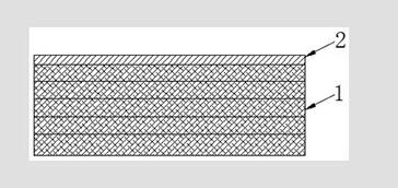
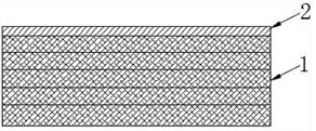
[0031] Embodiment: A laminated structure of housing materials for electronic products, including a composite material part 1, the composite material part is formed by bonding several layers of unit material structures, and each of the unit material structures is made of resin and a layer of plastic fiber layer Composition, the plastic fiber layer is at least one of carbon fiber layer, glass fiber layer and Kevlar fiber layer, the resin is one of thermosetting resin and thermoplastic resin, and the composite material part has relative An outer surface and an inner surface, a plastic film 2 is formed on the outer surface.

[0032] The plastic film is one of polycarbonate (PC) film, polyterephthalic acid (PET) film, polymethyl methacrylate (PMMA, also known as acrylic) film and polyamide (PA) film .

[0033] The thickness of the plastic film is 38 μm˜125 μm.

[0034] The surface of the plastic film may have a pattern.

[0035] The composite material part is one of the followin...


PUM

PropertyMeasurementUnit
thicknessaaaaaaaaaa

Abstract

The invention discloses an electronic product shell material laminating structure and a manufacture method thereof. One layer of plastic film covers on the laminating structure of the composite material; and the composite material covered with the plastic film is laminated, solidified and shaped by pressurizing and heating a die to form the electronic product shell material laminating structure composed of the composite material part and the plastic film so as to simplify the subsequent surface treatment process. The surface of the electronic product shell material laminating structure only needs to be polished once, supplemented with soil or sprayed, or the product can achieve a final finished product effect without polishing, supplementing with oil and spraying, and the surface treatment cost is lowered.

Description

technical field [0001] The invention belongs to the field of shell materials of electronic products, and in particular relates to a material lamination structure and a manufacturing method of the shell of electronic products which can simplify the surface treatment process. Background technique [0002] The composite materials used in the existing electronic product shells generally have many flaws and problems on the surface of the product after the surface treatment process is formed. Spraying bridging coatings to ensure the interlayer adhesion between coatings leads to complex surface treatment process and high cost of composite materials, which is not conducive to the increase of its market share, and hinders its application and development to a certain extent. Contents of the invention [0003] In order to overcome the above defects, the present invention provides a laminated structure of housing materials for electronic products and a manufacturing method thereof. Th...

Claims


Application Information

Patent Timeline
Patent Type & Authority Applications(China)
IPC IPC(8): B32B27/04B32B37/06B32B38/08
Inventor 洪健翎
Owner KUSN TONG YIN INDAL ELECTRONICS MAKING
Why Eureka
Try Eureka