
Photon-assisted porous silicon electrochemical etching tank

A light-assisted, etch tank technology, applied in the electrolysis process, electrolysis components, etc., can solve the problems that the quality and efficiency of the double-slot electrochemical corrosion process cannot be guaranteed, and the hole concentration of the silicon wafer to be etched is difficult to control, etc., to achieve guaranteed The effect of quality and efficiency, stable chemical properties

Inactive Publication Date: 2015-07-08
HANGZHOU SILAN INTEGRATED CIRCUIT
View PDF7 Cites 0 Cited by
  • Summary
  • Abstract
  • Description
  • Claims
  • Application Information

AI Technical Summary

Problems solved by technology

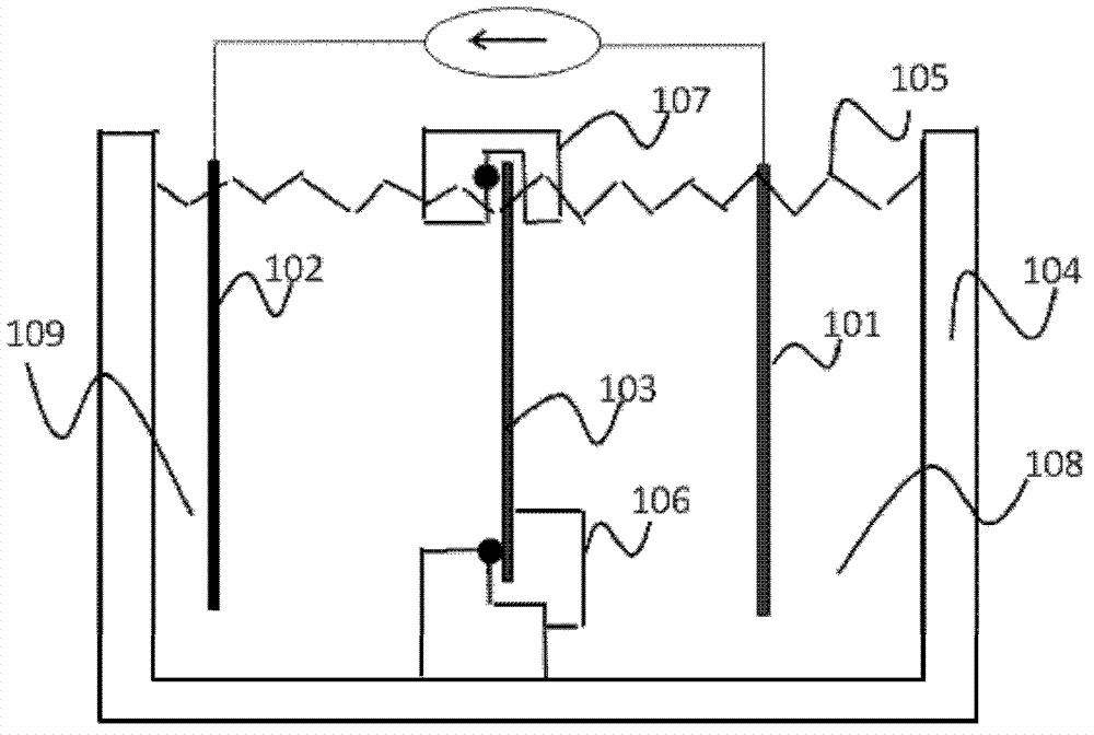
[0010] The object of the present invention is to provide a light-assisted electrochemical etching cell for porous silicon to solve the problem that the hole concentration in the silicon wafer to be etched is difficult to control in the prior art double cell electrochemical etching process, thus causing double cell electrochemical corrosion. The quality and efficiency of the process cannot be guaranteed

Method used


Image

  • Photon-assisted porous silicon electrochemical etching tank
  • Photon-assisted porous silicon electrochemical etching tank
  • Photon-assisted porous silicon electrochemical etching tank

Examples


Embodiment Construction

[0034] The light-assisted porous silicon electrochemical etching tank proposed by the present invention will be further described in detail below in conjunction with the accompanying drawings and specific examples. Advantages and features of the present invention will be apparent from the following description and claims. It should be noted that all the drawings are in a very simplified form and use imprecise scales, and are only used to facilitate and clearly assist the purpose of illustrating the embodiments of the present invention.

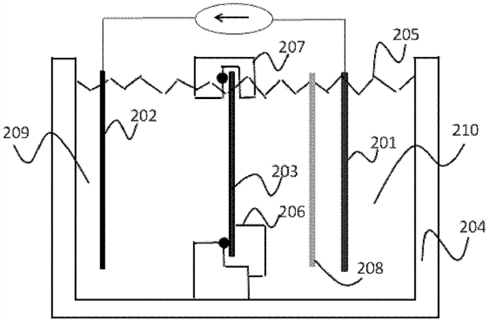
[0035] Please refer to figure 2 , which is a schematic structural view of a light-assisted electrochemical etching cell for porous silicon according to an embodiment of the present invention. Such as figure 2 As shown, the photo-assisted electrochemical etching cell of porous silicon comprises:

[0036] tank body 204;

[0037] A fixture for fixing the silicon wafer 203 to be etched in the tank body 204;

[0038] An electrode located in ...


PUM

PropertyMeasurementUnit
diameteraaaaaaaaaa
thicknessaaaaaaaaaa

Abstract

The invention provides a photon-assisted porous silicon electrochemical etching tank which comprises a tank body, a fixing support, electrodes and a photon-assisted mechanism. The fixing support, the electrodes and the photon-assisted mechanism are arranged in the tank body; the fixing support is used for fixing a silicon chip to be etched; the electrodes comprises a cathode and an anode, and the cathode and the anode are fixed on two sides of the fixing support respectively; and the photon-assisted mechanism is arranged between the fixing support and the cathode, used for providing illumination for the silicon chip to be etched, and light source of the photon-assisted mechanism is sealed in transparent polycarbonate (PC) plastic which has a grooved gate structure to facilitate flow of etching solution. During a double groove electrochemical etching process, the photon-assisted mechanism between the cathode and the silicon chip to be etched in the tank body is used for irradiating the silicon chip to be etched directly at close range, therefore holes with a certain concentration are formed in the silicon chip to be etched, and quality and efficiency of the double groove electrochemical etching process are guaranteed.

Description

technical field [0001] The invention relates to the technical field of microelectronic mechanical equipment, in particular to a light-assisted porous silicon electrochemical etching tank. Background technique [0002] With the continuous development of micro-electro-mechanical systems (MEMS), porous silicon materials show a very broad application prospect in MEMS because of their good mechanical and thermal properties. First of all, the film layer based on porous silicon material can be prepared very thick, which can replace SiO2 and other materials in MEMS as a sacrificial layer, so that the microstructure can be quickly released without double-sided lithography when the microstructure is processed by bulk micromachining technology, and at the same time The problem that the distance between the structural layer and the substrate is too small can be well solved in the surface micromechanical technology; secondly, because porous silicon has a thermal conductivity far lower th...

Claims


Application Information

Patent Timeline
Patent Type & Authority Patents(China)
IPC IPC(8): C25F3/12C25F3/14C25F7/00
Inventor 闻永祥刘琛季峰江为团
Owner HANGZHOU SILAN INTEGRATED CIRCUIT
Learn More