

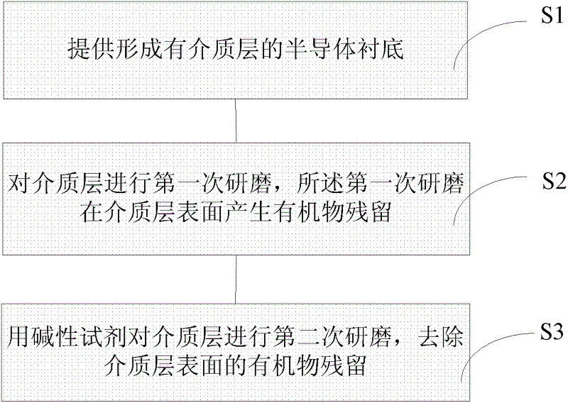
Chemical mechanical lapping method
A grinding method and chemical mechanical technology, which is applied in the field of semiconductor technology, can solve the problems of insufficient cleaning effect, insignificant effect, and no better solution, etc., and achieve the effect of removing organic residues
- Summary
- Abstract
- Description
- Claims
- Application Information
AI Technical Summary
Problems solved by technology
Method used
Image

Examples
Embodiment 1
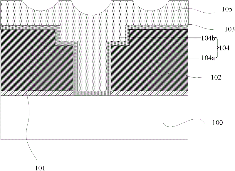
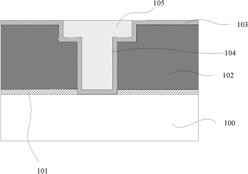
[0037] Embodiment 1: Reference Figure 2 to Figure 4 Schematic diagram of chemical mechanical polishing during formation of dual damascene structures shown.
[0038] Specifically, refer to figure 2 As shown, first, a semiconductor substrate 100 is provided, and the semiconductor substrate 100 contains a metal wiring layer ( figure 2 not shown in); forming a cover layer 101 on the semiconductor substrate 100, the cover layer 101 covering the metal wiring layer; and forming a dielectric layer 102 on the cover layer 101 by a chemical vapor deposition (CVD) method, the medium The material of layer 102 is silicon dioxide, low-K (dielectric constant) material, and the like.
[0039] In this embodiment, the covering layer 101 can prevent the metal wiring in the semiconductor substrate 100 from diffusing into the dielectric layer 102, and can also prevent the metal wiring in the semiconductor substrate 100 from being etched during the etching process.
[0040] continue to refer ...
PUM
| Property | Measurement | Unit |
|---|---|---|
| diameter | aaaaa | aaaaa |
Abstract
Description
Claims
Application Information