Shielded PCB

A technology for printed circuit boards and shielding films, applied to printed circuits, printed circuit components, circuit devices, etc., can solve the problems of increased area of ​​shielded printed circuit boards and limited design freedom, so as to maintain the shielding effect and improve design Degree of freedom, reliable equipotential maintenance effect

Active Publication Date: 2016-05-04
TATSUTA ELECTRICWIRE & CABLE
View PDF6 Cites 0 Cited by
  • Summary
  • Abstract
  • Description
  • Claims
  • Application Information

AI Technical Summary

Problems solved by technology

However, when a grounding component is provided on the outside of the shield printed circuit board 100, for example, there will be a problem that the area of ​​the shielded printed circuit board will be reduced due to the need to provide wiring for connecting the reinforcing member 135 and the grounding component. will increase accordingly, resulting in limited design freedom

Method used


Image

  • Shielded PCB
  • Shielded PCB
  • Shielded PCB

Examples


Embodiment Construction

[0036] Hereinafter, preferred embodiments of the present invention will be described with reference to the drawings.

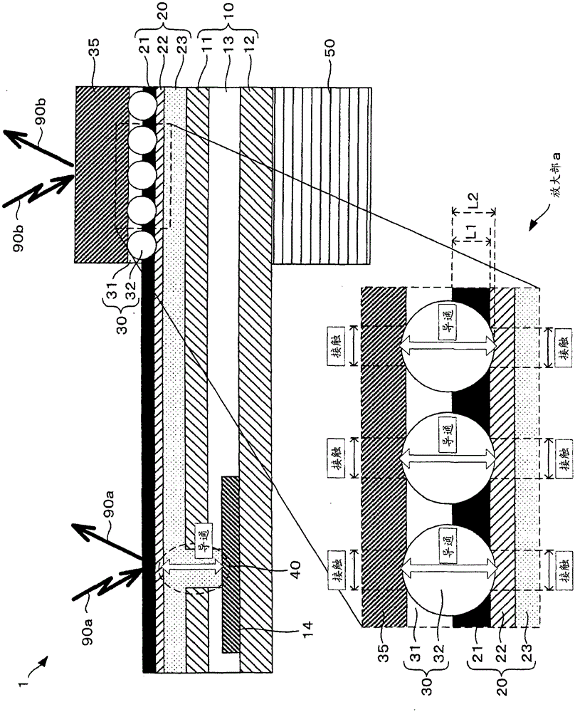
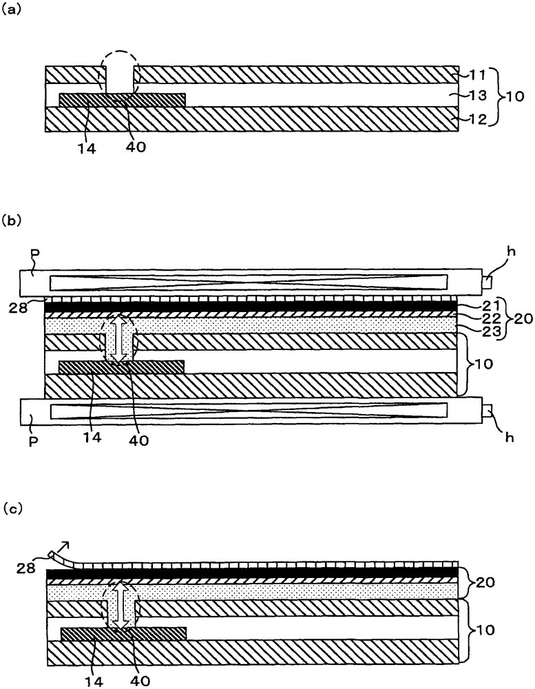
[0037] (Overall structure of shielded printed circuit board 1)

[0038] First, use figure 1 The shield printed wiring board 1 of this embodiment will be described. Such as figure 1 As shown, the shielded printed circuit board 1 includes a printed circuit board 10 , a shielded film 20 and a reinforcing member 35 . Furthermore, an electronic component 50 is connected to a mounting portion provided on the lower surface of the printed circuit board 10 . In addition, the shielding film 20 is provided on the printed circuit board 10 and covers a part or the whole of an area opposite to a mounting portion where the electronic component 50 is connected. Thereby, noises such as electromagnetic waves 90b radiated from the outside to the mounting portion of the electronic component 50 are shielded by the shielding film 20 .

[0039] Furthermore, the reinforcing me...


PUM


Abstract

The invention relates to a shielded type printed circuit board, which comprises a printed circuit board, a shielding film and a strengthening component. The printed circuit board comprises a base component and an insulation film, wherein a circuit pattern used for ground connection is formed on the base component, the insulation film is arranged on the base component, the circuit pattern used for ground connection is covered by the insulation film, and an electronic component is connected at the installation place of the lower surface of the base component. The shielding film arranged on the printed circuit board comprises an electric conduction layer and an insulation layer, wherein the electric conduction layer is equipotential with the circuit pattern used for ground connection, and the electric conduction layer is arranged on the printed circuit board and is used for covering a part of a zone or the whole zone opposite to the installation place; and the insulation layer is arranged at the electric conduction layer. The strengthening component has electroconductivity and is arranged on the shielding film at the zone opposite to the installation place. The strengthening component is jointed with the insulation layer by electric conductivity cement containing spherical electric conductivity particles. The thickness of the insulation layer is less than the raising length of the electric conductivity particles from the electric conductivity cement under the joint state of the electric conductivity cement and the insulation layer, and the electric conductivity particles are in contact with the electric conduction layer under the joint state of the electric conductivity cement and the insulation layer.

Description

technical field [0001] This invention relates to shielded printed circuit boards for cellular phones, computers and the like. Background technique [0002] Conventionally, electronic devices such as mobile phones and computers have been easily affected by noise from motherboards or external electromagnetic waves due to miniaturization and high-speed processing. Therefore, there is an increasing demand for printed circuit boards having shielding films that shield noise such as electromagnetic waves. In addition, since such printed circuit boards are used in connection with electronic components used in mobile phones, computers, etc., due to bending during use, etc., the mounting portion where the electronic components are mounted may be twisted and deformed. Therefore, the above-mentioned problem is solved by providing a reinforcing member at a position opposite to a mounting portion where the electronic component is mounted. [0003] For example, Figure 5 is a schematic d...

Claims


Application Information

Patent Timeline
Patent Type & Authority Patents(China)
IPC IPC(8): H05K1/02H05K9/00
CPCH05K1/0218H05K1/182
Inventor 森元昌平田岛宏上农宪治
Owner TATSUTA ELECTRICWIRE & CABLE
Why Eureka
Try Eureka