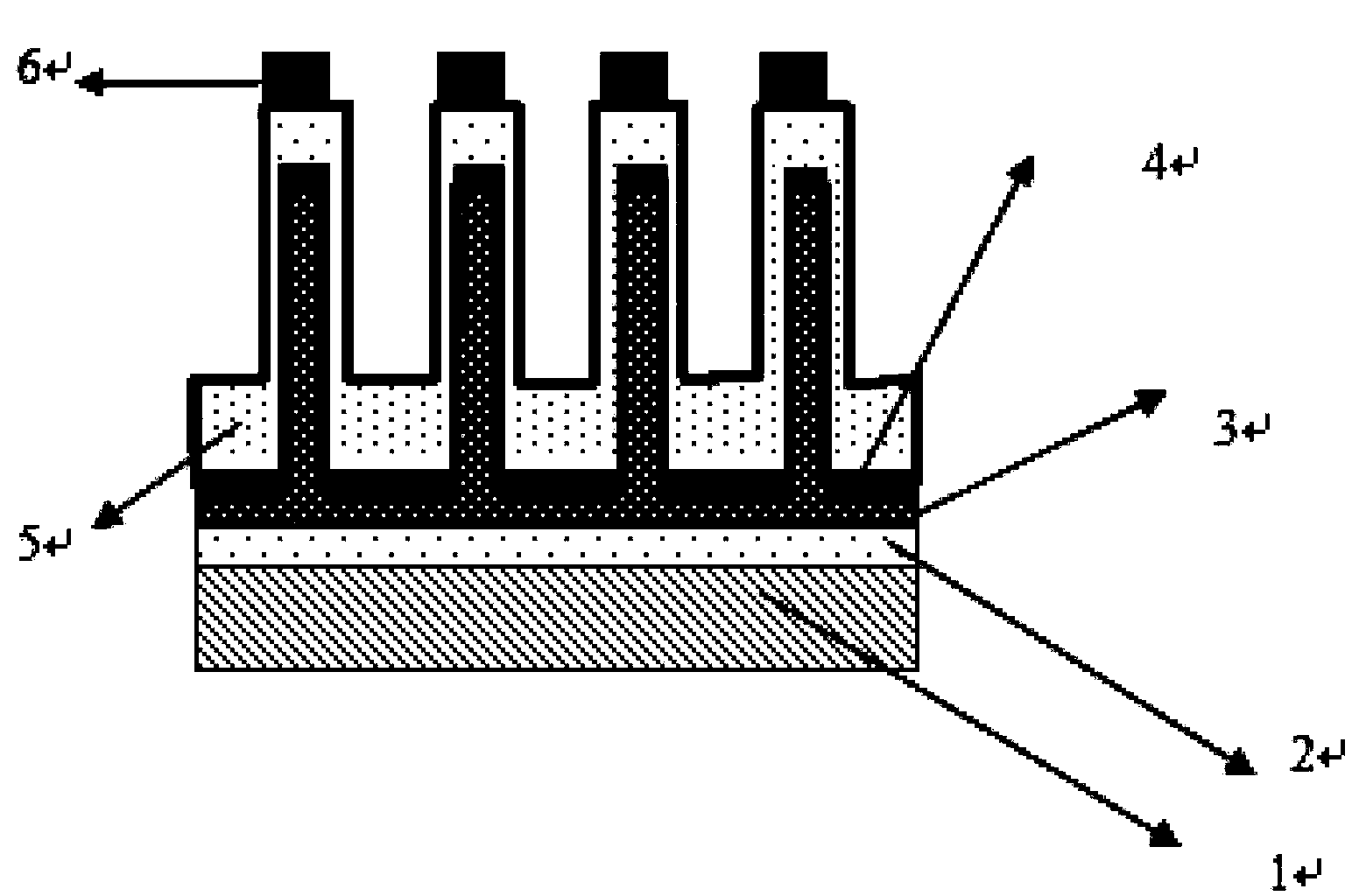
Nanometer structure copper zinc tin sulfide (CZTS) film photovoltaic cell and preparation method of nanometer structure CZTS film photovoltaic cell
A thin-film photovoltaic cell and nanostructure technology, which is applied to photovoltaic power generation, circuits, electrical components, etc., can solve the problems of low conversion efficiency of CZTS thin-film solar photovoltaic cells, and achieve the effects of high photoelectric conversion efficiency, cost reduction and simple preparation process.
- Summary
- Abstract
- Description
- Claims
- Application Information
AI Technical Summary
Problems solved by technology
Method used
Image
Examples
Embodiment 1
[0047] A nanostructure CZTS thin film photovoltaic cell, prepared by the following steps:
[0048] (1) Take the ceramics, wash them with 1mol / L NaOH solution and 1mol / L hydrochloric acid solution in turn, then ultrasonically clean them with absolute ethanol and deionized water in turn, and then sputter a layer of ITO on the ceramic substrate. The thickness is 700nm (ITO glass can also be used);
[0049] (2) Sputter a layer of copper film with a thickness of 1um on the substrate after sputtering deposition of ITO (ITO glass can also be selected);
[0050] (3) Mix the substrate sputtered with copper film with hydrogen sulfide / oxygen mixed gas (the volume ratio of the two is 1:4), and vulcanize at 18°C for 18 hours to form a cuprous sulfide nanowire array;
[0051] (4) Put the substrate on which the cuprous sulfide nanowire array has been formed into 0.5 mol / L hydrochloric acid aqueous solution to dissolve the surface oxide layer;
[0052] (5) The product of step (4) was soak...
Embodiment 2
[0060] A nanostructure CZTS thin film photovoltaic cell, prepared by the following steps:
[0061] (1) Take the silicon wafer, wash it with 1mol / L NaOH solution and 1mol / L hydrochloric acid solution in turn, then ultrasonically clean it with absolute ethanol and deionized water in turn, and then sputter a layer of Al on the silicon wafer substrate, The thickness of Al is 800nm;
[0062] (2) Sputter a layer of copper film with a thickness of about 1um on the substrate after Al is deposited;
[0063] (3) Mix the substrate sputtered with copper film with hydrogen sulfide / oxygen mixed gas (the volume ratio of the two is 1:2), and vulcanize at 20°C for 14 hours to form a subnano-sulfide array;
[0064] (4) Put the substrate on which the copper sulfide nanowire array was formed into 1mol / L hydrochloric acid aqueous solution to dissolve the surface oxide layer;
[0065] (5) Put the product of step (4) on the rotating substrate holder of the magnetron sputtering apparatus, co-sputte...
Embodiment 3
[0072] A nanostructure CZTS thin film photovoltaic cell, prepared by the following steps:
[0073] (1) Electron beam evaporation of a layer of W on the newly cut mica substrate, the thickness of W is 800nm;
[0074] (2) Evaporate a layer of copper film with a thickness of about 1um on the substrate after electron beam evaporation of W;
[0075] (3) Mix the substrate with the evaporated copper film with hydrogen sulfide / oxygen mixed gas (the volume ratio of the two is 1:2), and vulcanize at 22°C for 12 hours to form a copper sulfide nanowire array;
[0076] (4) Put the substrate on which the copper sulfide nanowire array was formed into 1mol / L hydrochloric acid aqueous solution to dissolve the surface oxide layer;
[0077] (5) Put the product of step (4) on the rotating substrate holder, layer-evaporate Zn, Sn, S, and then 2 Under gas protection, p-type semiconductor nanowire arrays were obtained after heat treatment at 600°C for 15 hours;
[0078] (6) After the evaporation ...
PUM
| Property | Measurement | Unit |
|---|---|---|
| thickness | aaaaa | aaaaa |
| thickness | aaaaa | aaaaa |
| thickness | aaaaa | aaaaa |
Abstract
Description
Claims
Application Information
