Check patentability & draft patents in minutes with Patsnap Eureka AI!

TFT-LCD (thin film transistor liquid crystal display) array substrate and manufacturing and repairing methods thereof

A technology for array substrates and manufacturing methods, which is applied in the field of TFT-LCD array substrates and its manufacture and repair, and can solve problems such as difficult repair of data lines

Inactive Publication Date: 2012-08-22
BOE TECH GRP CO LTD +1
View PDF5 Cites 5 Cited by
  • Summary
  • Abstract
  • Description
  • Claims
  • Application Information

AI Technical Summary

Problems solved by technology

[0005] The invention provides a TFT-LCD array substrate and its manufacturing and repairing methods, which are used to solve the problem that the data line of the array substrate in the prior art is not easy to repair when it fails

Method used


Image

  • TFT-LCD (thin film transistor liquid crystal display) array substrate and manufacturing and repairing methods thereof
  • TFT-LCD (thin film transistor liquid crystal display) array substrate and manufacturing and repairing methods thereof
  • TFT-LCD (thin film transistor liquid crystal display) array substrate and manufacturing and repairing methods thereof

Examples


Embodiment Construction

[0024] Embodiments of the present invention provide a TFT-LCD array substrate and methods for manufacturing and repairing the same, which can solve the problem in the prior art that the data lines of the array substrate are not easy to repair when they fail.

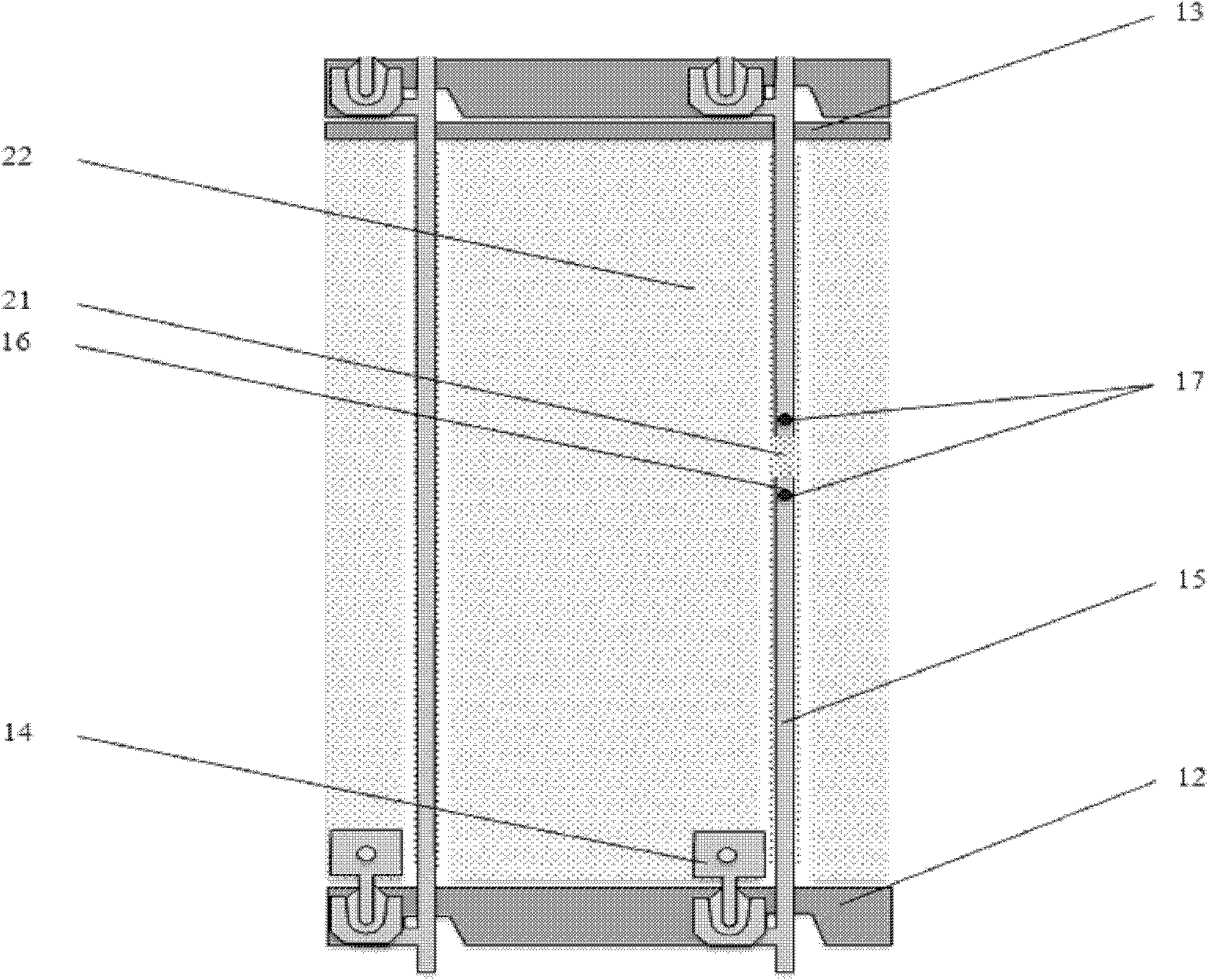
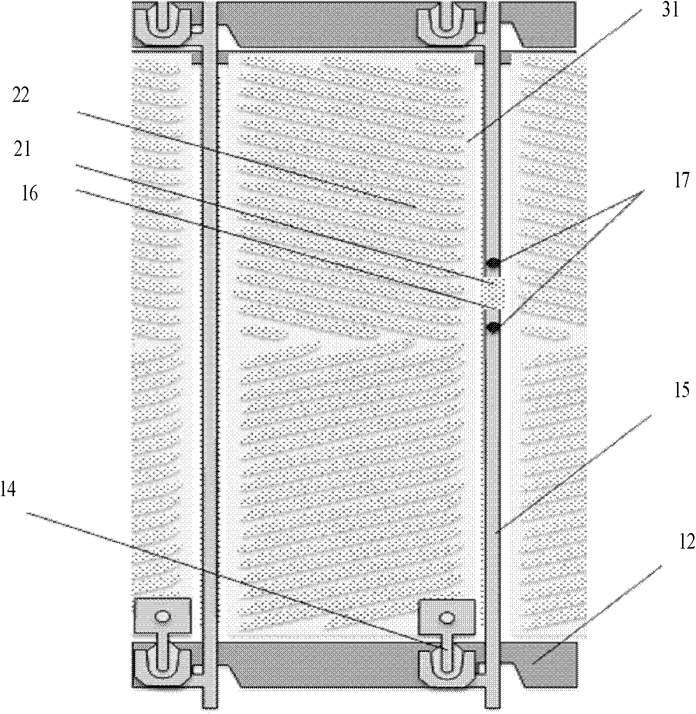
[0025] An embodiment of the present invention provides a TFT-LCD array substrate, including:

[0026] The substrate and the first transparent conductive film, the gate layer, the gate insulating layer, and the source-drain electrode layer are sequentially formed on the substrate from bottom to top, and a passivation layer and a second transparent conductive layer may be further included on the source-drain electrode layer. conductive film,

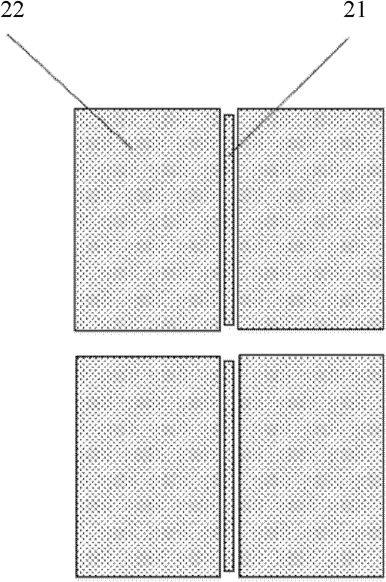
[0027] Wherein, the gate layer includes gate lines and common electrode lines, and the source-drain electrode layer includes data lines and transistors, then the first transparent conductive film includes at least a first portion and a second portion that are not in contact with each...


PUM


Abstract

The invention discloses a TFT-LCD (thin film transistor liquid crystal display) array substrate which comprises a substrate, and a first transparent conductive film, a grid layer, a gate insulating layer and a source drain electrode layer which, from top to bottom, are sequentially formed on the substrate, wherein the grid layer comprises a grid line and a common electrode wire, the source drain electrode layer comprises a data line and a transistor, the first transparent conductive film at least comprises a first part and a second part which are not contacted with each other, the first part is arranged below an area at which the data line is located, and not contacted with the grid line and the common electrode wire. According to the array substrate disclosed by the embodiment of the invention, when the data line is open-circuit, the part of the conductive film and the data line can be welded together directly by using a laser welding technology, thereby achieving the purpose of repairing the data line.

Description

technical field [0001] The invention relates to the field of thin film transistor liquid crystal display, in particular to a TFT-LCD array substrate and a manufacturing and repairing method thereof. Background technique [0002] Thin Film Transistor Liquid Crystal Display (TFT-LCD) has the advantages of small size, low power consumption, and no radiation, and occupies a dominant position in the current flat panel display market. Advanced-Super Dimensional Switching (AD-SDS) generates a fringe electric field through the electrodes between pixels in the same plane, so that the aligned liquid crystal molecules between the electrodes and directly above the electrodes can be in the plane direction, that is, parallel to the substrate. The direction produces a rotation conversion, which improves the light transmission efficiency of the liquid crystal layer while increasing the viewing angle. [0003] The AD-SDS type TFT-LCD array substrate in the prior art generally includes the f...

Claims


Application Information

Patent Timeline
IPC IPC(8): G02F1/1362G02F1/1368G02F1/13H01L27/02H01L21/77
CPCH01L27/124G02F1/136259H01L29/41733
Inventor 周保全
Owner BOE TECH GRP CO LTD
Features
  • R&D
  • Intellectual Property
  • Life Sciences
  • Materials
  • Tech Scout
  • Unparalleled Data Quality
  • Higher Quality Content
  • 60% Fewer Hallucinations
Learn More