

Shift register unit, shift register circuit, array substrate and display device
A shift register and circuit technology, applied in the fields of array substrates and display devices, shift register circuits, and shift register units, can solve the problems of unfavorable working life of shift register circuits and long bias voltage action time, etc.
- Summary
- Abstract
- Description
- Claims
- Application Information
AI Technical Summary
Problems solved by technology
Method used
Image

Examples
Embodiment Construction
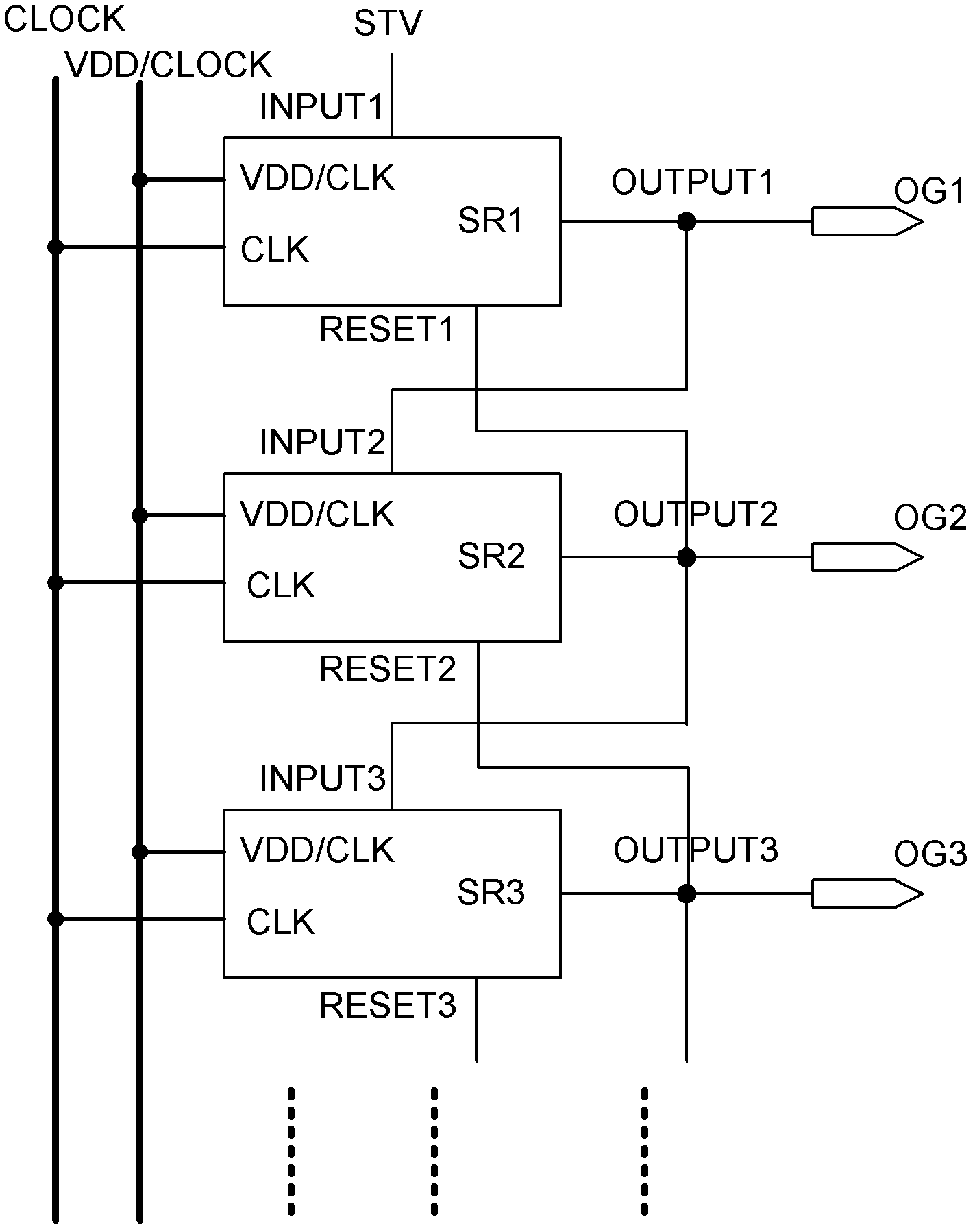
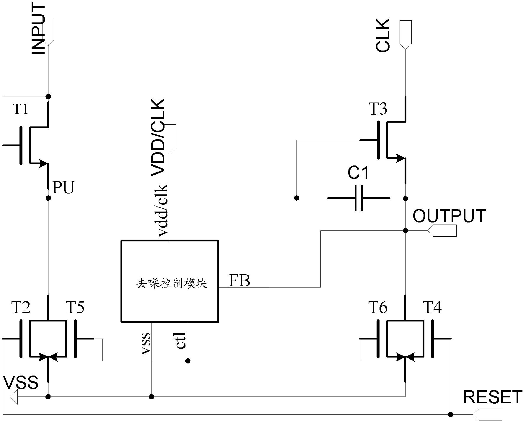
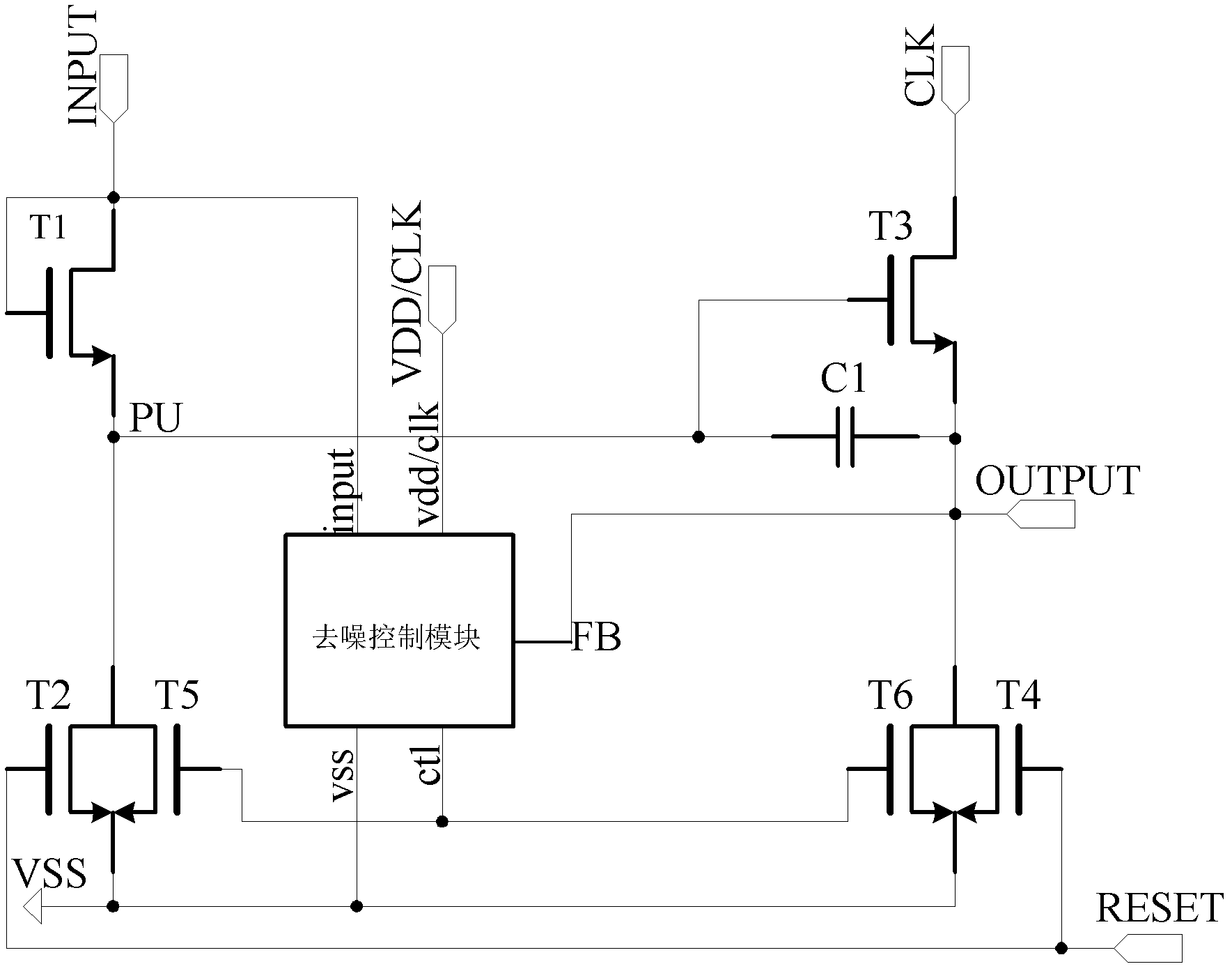
[0044] The following will clearly and completely describe the technical solutions in the embodiments of the present invention with reference to the accompanying drawings in the embodiments of the present invention. Obviously, the described embodiments are only some of the embodiments of the present invention, not all of them. Based on the embodiments of the present invention, all other embodiments obtained by persons of ordinary skill in the art without making creative efforts belong to the protection scope of the present invention.
[0045] The transistors used in all embodiments of the present invention can be thin film transistors or field effect transistors or other devices with the same characteristics. Since the source and drain of the transistors used here are symmetrical, there is no difference between the source and the drain. of. In the embodiment of the present invention, in order to distinguish the two poles of the transistor except the gate, one pole is called the...
PUM
 Abstract
Description
Claims
Application Information