Optical-interface patterning for radiation detector crystals
A technology of radiation detectors and crystals, which can be used in radiation measurement, radiation intensity measurement, X/γ/cosmic radiation measurement, etc., and can solve problems such as expensive, low collection rate, and reduced light collection
- Summary
- Abstract
- Description
- Claims
- Application Information
AI Technical Summary
Problems solved by technology
Method used
Image
Examples
Embodiment Construction
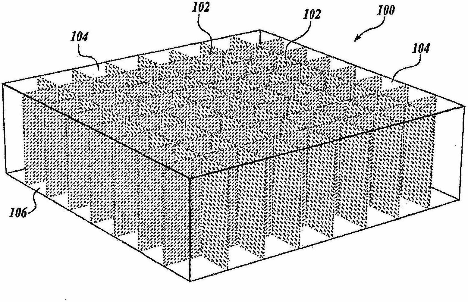
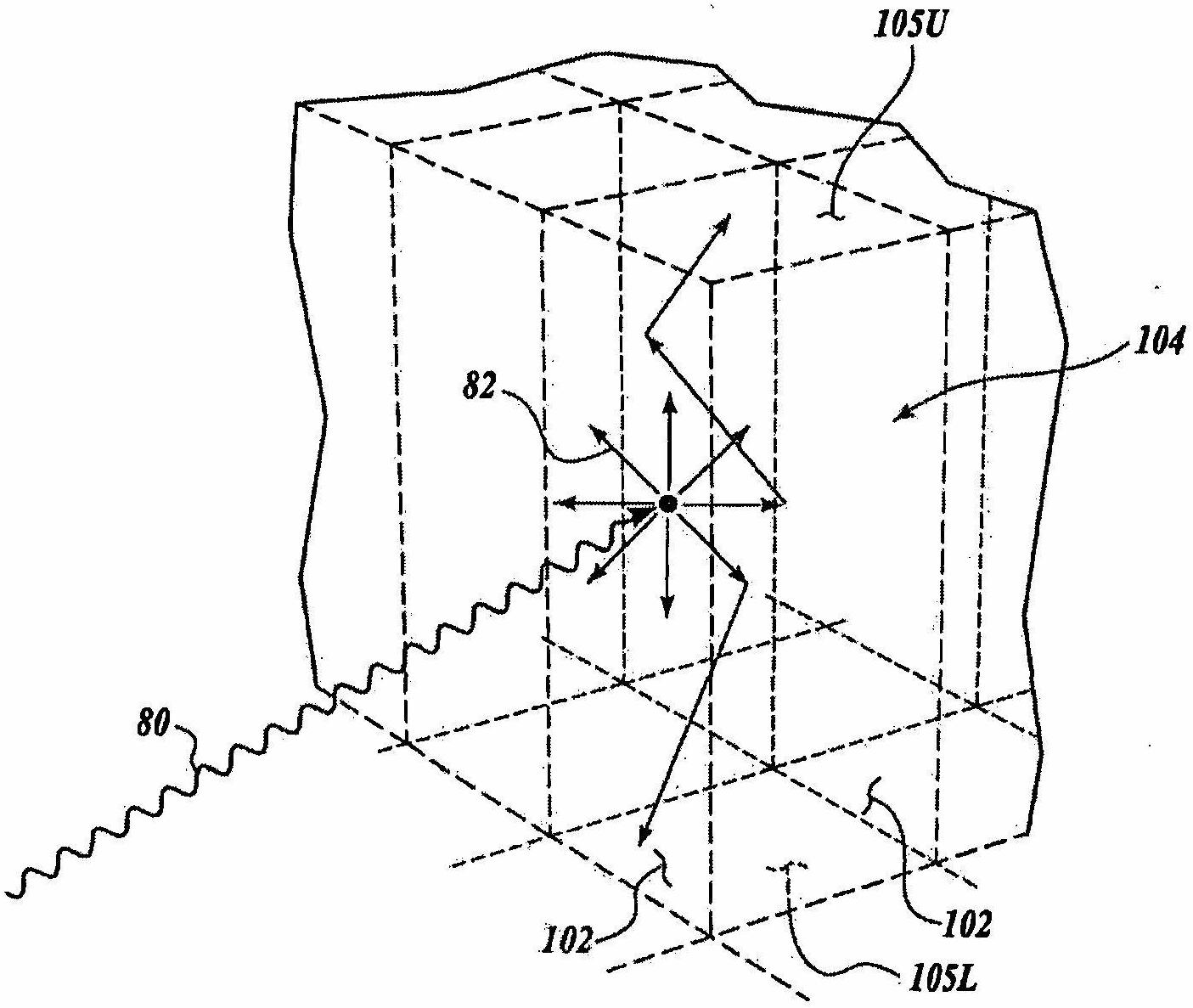
[0039] We present a novel application for subsurface laser engraving (SSLE), where SSLE is used to generate point-like defects in the inner regions of optical elements, such as scintillation crystals. These defects are configured to control the transport of low-energy photons within the optical device. For example, and as discussed in more detail below, arrays of point defects produced by SSLEs can function as reflective optical boundaries or interfaces in optical elements, such as scintillators, optical waveguides, or lenses. The pattern and density of point defects and the characteristics of individual point defects determined by the SSLE process can be used to control the transmission and / or distribution of light in the optical unit. Furthermore, these properties of point defect patterns, which can vary as a function of position, make light transport across the interface unstable. Alternatively or additionally, the distribution of point defects introduced by the volume can...
PUM
 Abstract
Description
Claims
Application Information


