Digital delay device

A delay device, digital technology, applied in the direction of electrical components, automatic power control, etc., can solve problems such as large clock jitter noise, and achieve the effect of reducing jitter noise

Active Publication Date: 2012-09-12
LOONGSON TECH CORP
View PDF7 Cites 17 Cited by
  • Summary
  • Abstract
  • Description
  • Claims
  • Application Information

AI Technical Summary

Problems solved by technology

[0007] The present invention provides a digital delay device to solve the relatively large clock jitter noise caused by the large number of de...

Method used


Image

  • Digital delay device
  • Digital delay device
  • Digital delay device

Examples


Embodiment 1

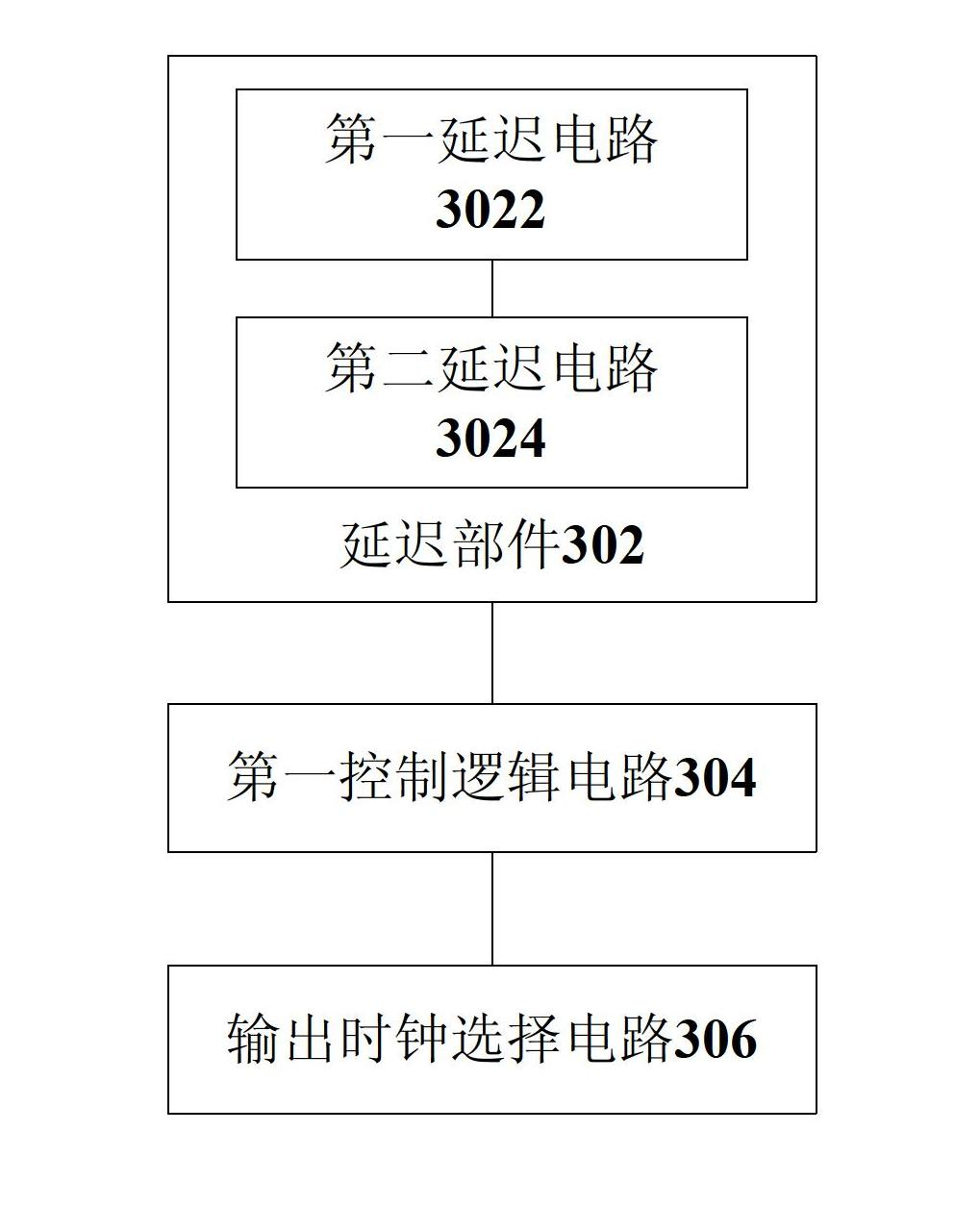
[0038] The present invention provides a digital delay device, specifically, such as image 3As shown, the device includes: a delay unit 302, and the delay unit 302 includes a first delay circuit 3022 and a second delay circuit 3024, wherein the first delay circuit 3022 and the second delay circuit 3024 are used to respectively process digital signals that are differential signals signal, the input signal of the first delay circuit 3022 and the input signal of the second delay circuit 3024 are mutually differential signals, the output signal of the first delay circuit 3022 and the output signal of the second delay circuit 3024 are mutually differential signals, and the first delay circuit 3022 and the second delay circuit 3024 are all formed by cascading delay units; the first control logic circuit 304 is used to control the first delay circuit 3022 and the second delay circuit 3024 to output the first clock signal and the second clock signal respectively; the output clock The ...

Embodiment 2

[0046] Figure 10 A schematic diagram showing a preferred structure of the digital delay device of the present invention, the components of the delay chain include a differential chain, a control logic circuit, a coupling unit, and an output clock selection circuit, wherein the differential chain includes two chains, respectively called positive The chain (the first delay circuit) and the anti-chain (the second delay circuit) are composed of cascaded differential delay units in a ladder structure. The input clock is a pair of differential clock signals, and the output clock is a clock signal delayed by a differential chain delay unit and a selection circuit. The working principle of each component is as follows:

[0047] Delay unit: built with N-level non-logic gates for delay time, including two working states: the first working state and the second working state, the working principle of which has been described in Embodiment 1, and will not be repeated here.

[0048] The ...


PUM


Abstract

The invention discloses a digital delay device, which comprises a delay part, a first control logic circuit and an output clock selection circuit, wherein the delay part comprises a first delay circuit and a second delay circuit, which are used for processing digital signals respectively, and the digital signals are differential signals of each other; the first control logic circuit is used for controlling the first and second delay circuits to output a first clock signal and a second clock signal respectively; and the output clock selection circuit is used for outputting a third clock signal according to the first clock signal and/or the second clock signal. The problem that a great number of delay units of a delay chain are required to cause loud clock jitter noise when a digital delay locked loop is required to have maximum delay time in related technologies is solved, and the effect of lowering the clock jitter noise is achieved.

Description

technical field [0001] The invention relates to a delay-locked loop circuit in a high-speed circuit system, in particular to a digital delay device. Background technique [0002] Delay-locked loops have been widely adopted for clock deskew and clock generation in high-speed systems. Delay-locked loops can be roughly divided into two types: analog delay-locked loops and digital delay-locked loops. Although analog delay-locked loops have better clock delay accuracy and stronger anti-jitter capability, they are very sensitive to semiconductor process changes, and it is more difficult to transplant under different processes. However, the digital delay-locked loop is very suitable for transplantation under different processes. Therefore, even if the semiconductor technology is constantly improving and updating, the digital delay-locked loop can complete the process transplantation of the circuit in a short period of time with less manpower. With the continuous shrinking of the...

Claims


Application Information

Patent Timeline
IPC IPC(8): H03L7/08
Inventor 陈帅李昊钟石强
Owner LOONGSON TECH CORP
Why Eureka
Try Eureka