Silk screen print positioning equipment and method for photovoltaic solar silicon chip

A photovoltaic solar energy and screen printing technology, which is applied in the direction of screen printing machines, printing machines, printing machines, etc., can solve the problems of expanding the field of vision and increasing the height of the installed camera, and achieves simple equipment structure, simple mechanical structure, and guaranteed positioning The effect of registration

Inactive Publication Date: 2012-09-19
HUAZHONG UNIV OF SCI & TECH +1
View PDF7 Cites 29 Cited by
  • Summary
  • Abstract
  • Description
  • Claims
  • Application Information

AI Technical Summary

Problems solved by technology

However, this method still has the following defects: First, although visual detection of silicon wafer fragments can achieve a certain effect, in actual production, it is not easy to cause damage during the transmission of fragments, and more silicon wafers are damaged during the printing process. Due to the dark lines caused by the pressure of the scraper, the feasibility of visual detection of dark lines is very poor; secondly, the size of silicon wafers...

Method used


Image

  • Silk screen print positioning equipment and method for photovoltaic solar silicon chip
  • Silk screen print positioning equipment and method for photovoltaic solar silicon chip
  • Silk screen print positioning equipment and method for photovoltaic solar silicon chip

Examples


Embodiment Construction

[0039] In order to make the object, technical solution and advantages of the present invention clearer, the present invention will be further described in detail below in conjunction with the accompanying drawings and embodiments. It should be understood that the specific embodiments described here are only used to explain the present invention, not to limit the present invention.

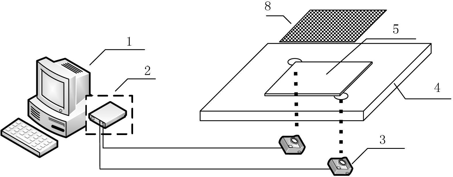
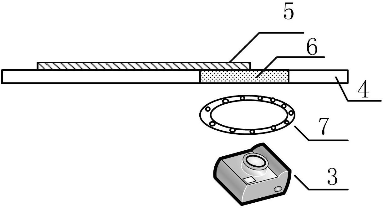
[0040] figure 1 It is a schematic diagram of the overall structure of the solar silicon wafer screen printing positioning device according to the present invention, figure 2 yes figure 1 Partial enlarged view of structural components such as camera device, light source and lens shown in . Such as figure 1 and figure 2 As shown, the screen printing positioning equipment for photovoltaic solar silicon wafers according to the present invention mainly includes a carrying platform 4, a camera device 3, a light source 7, and corresponding positioning and calibration devices. The carrying platform ...


PUM


Abstract

The invention discloses silk screen print positioning equipment and a silk screen print positioning method for a photovoltaic solar silicon chip. The method comprises the following steps of: arranging an image pickup device at two opposite angle positions corresponding to a silicon chip and a silk screen respectively, and performing a predetermined step of the image pickup device; shooting opposite angle position images of the silicon chip and the silk screen by using the image pickup device; acquiring the shot position images, acquiring position characteristic parameters of the silicon chip and the silk screen, which comprise geometric centers and angles, correspondingly calculating a position deviation between the silicon chip and the silk screen, and introducing a compensation deviation according to a target position to acquire a comprehensive deviation; and adjusting the position and the angle of the silk screen relative to the silicon chip according to the calculated comprehensive deviation to finish a silk screen print positioning process of the photovoltaic solar silicon chip. According to the equipment and the method, the position deviation between the silk screen and the silicon chip can be measured by a simple and compact structure, and high accuracy of measurement and print positioning can be ensured; and simultaneously, the equipment and the method have the advantages that the equipment and the method are convenient to operate, high in interference resistance, stable and reliable.

Description

technical field [0001] The invention belongs to the field of solar cell manufacturing, and more specifically relates to a screen printing positioning device for photovoltaic solar silicon wafers and a corresponding positioning method. Background technique [0002] Photovoltaic solar wafers are the core part of the solar power generation system, and also the most valuable part of the solar power generation system. The role of photovoltaic solar silicon wafers is to convert solar energy into electrical energy, and the electrical energy is sent to storage for storage, or directly used to drive loads. The quality and cost of photovoltaic solar silicon wafers will directly determine the quality and cost of the entire solar power generation system. For the basic electrodes of photovoltaic solar silicon wafers, the most commonly used production process is the screen printing method. The working principle of screen printing is to use the mesh part of the screen pattern to penetrat...

Claims


Application Information

Patent Timeline
IPC IPC(8): B41F15/14B41F33/00H01L31/18
CPCY02P70/50
Inventor 尹周平吉守龙权建洲钟强龙梁若陶文静熊有伦
Owner HUAZHONG UNIV OF SCI & TECH
Why Eureka
Try Eureka