Display device contact hole forming method

A display device and contact hole technology, which is applied in the manufacture of electrical components, circuits, semiconductor/solid-state devices, etc., can solve the problem of poor thickness and uniformity of patterned photoresist, large metal wiring overetching, and difficult to adjust etching speed, etc. problems, to avoid over-etching, simplify the etching speed, and optimize the etching process

Active Publication Date: 2015-03-18
SHANGHAI AVIC OPTOELECTRONICS
View PDF1 Cites 0 Cited by
  • Summary
  • Abstract
  • Description
  • Claims
  • Application Information

AI Technical Summary

Problems solved by technology

[0005] In the above two-step etching, due to the poor thickness and uniformity of the patterned photoresist above the shallow hole, it is difficult to control the time node in the middle of the first and second etching steps and the end time node of the second step etching , the etching rate is also more difficult to adjust due to the selection ratio of the etching gas. Therefore, a large amount of metal wiring overcut is prone to occur after etching

Method used


Image

  • Display device contact hole forming method
  • Display device contact hole forming method
  • Display device contact hole forming method

Examples


Embodiment 1

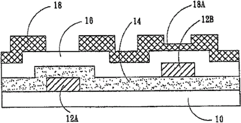
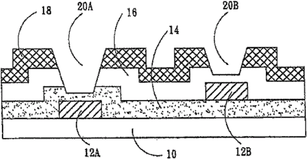
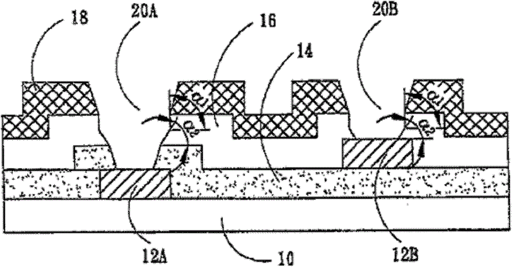
[0042] This embodiment provides a method for forming a contact hole of a display device, so as to optimize the etching process, enable better control of the etching process, and reduce the overcut amount of metal wiring during etching, such as figure 2 Shown method schematic flow chart, this method comprises the following steps:

[0043] Step S201, providing the substrate 10, the first metal layer 12A is formed on the substrate, the first metal layer 12A and the substrate 10 are covered with the insulating layer 14, the second metal layer 12B is formed on the insulating layer 14, and the second metal layer 12B does not overlap with the first metal layer 12A in the direction perpendicular to the substrate 10, see Figure 3A The schematic diagram of the device structure after forming the second metal layer 12B is shown, the second metal layer 12B and the insulating layer 14 are covered with a passivation layer 16, see Figure 3B As shown in the structural diagram, the passivat...


PUM

PropertyMeasurementUnit
thicknessaaaaaaaaaa

Abstract

The embodiment of the invention discloses a display device contact hole forming method which includes the following steps of: providing a substrate on which a first metal layer, an insulating layer, a second metal layer, a passivated layer and a patterning photoresist layer are sequentially formed; performing a first etching step to remove the entire thickness of the passivated layer and the partial thickness of the insulating layer above the first metal layer, and at the same time to remove the partial thickness of the corresponding halftone photoresist above the second metal layer; performing an ashing step to totally remove the corresponding halftone photoresist above the second metal layer; and performing a second etching step to remove the insulating layer retained in a deep hole above the first metal layer so as to expose the surface of the first metal layer and at the same time to remove the passivated layer retained in a shallow hole above the second metal layer so as to expose the surface of the second metal layer. The scheme of the invention can overcome the disadvantage that the uniformity of the remnant film of the photoresist is difficult to control, and the etching processes are optimized; the process of controlling the etching speed is simple; and over etching of the metal wirings can be avoided to the largest extent.

Description

Technical field: [0001] The invention relates to the technical field of display device manufacturing, in particular to a method for forming a contact hole of a display device. Background technique: [0002] In the TFT (Thin Film Transistor, thin film transistor) manufacturing process, the composition structure and area of ​​TFT are optimized. Among them, the metal wiring is divided into D (data, data) wiring and G (gate gate) wiring Two types, an insulating layer and a passivation layer are deposited between the metal wirings and between the metal wirings and the transparent electrode layer. In order to minimize interference to signals transmitted through wiring components, the insulating layer is usually formed of low dielectric material, contact holes are formed in the passivation layer and the insulating layer, and the metal wiring that transmits the same signal is usually passed through several contacts The contact hole connecting the D wiring and the transparent electr...

Claims


Application Information

Patent Timeline
Patent Type & Authority Patents(China)
IPC IPC(8): H01L21/768H01L21/311
Inventor 张建强张容李延辉康亮
Owner SHANGHAI AVIC OPTOELECTRONICS
Why Eureka
Try Eureka