Display device contact hole forming method
A technology for display devices and contact holes, which is applied in the manufacturing of electrical components, circuits, semiconductor/solid-state devices, etc. problems, to avoid over-etching, simplify the etching speed, and optimize the etching process
- Summary
- Abstract
- Description
- Claims
- Application Information
AI Technical Summary
Problems solved by technology
Method used
Image
Examples
Embodiment 1
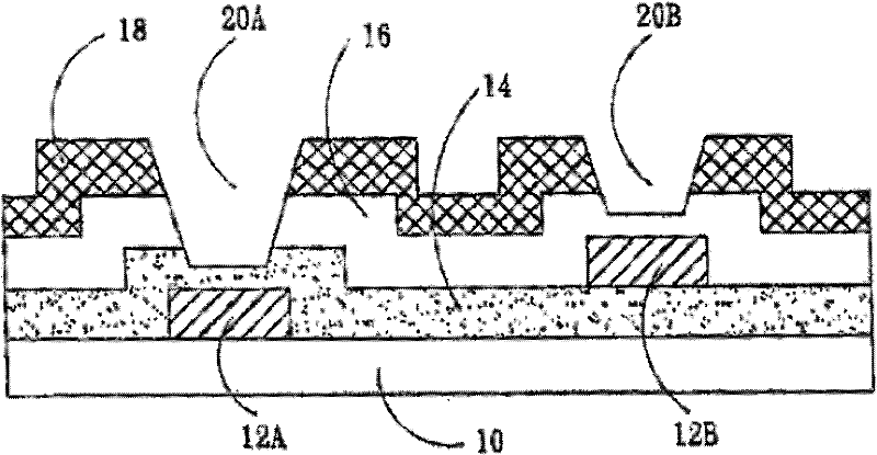
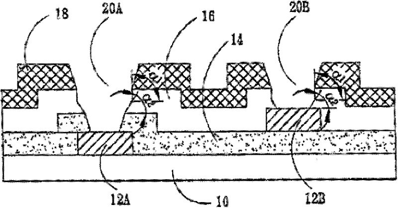
[0042] This embodiment provides a method for forming a contact hole of a display device, so as to optimize the etching process, enable better control of the etching process, and reduce the overcut amount of metal wiring during etching, such as figure 2 Shown method schematic flow chart, this method comprises the following steps:
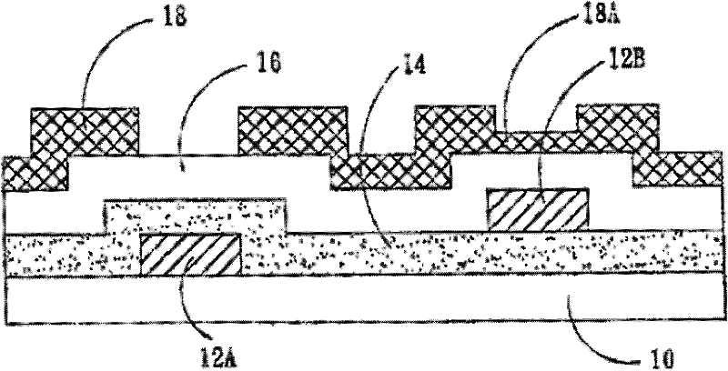
[0043] Step S201, providing the substrate 10, the first metal layer 12A is formed on the substrate, the first metal layer 12A and the substrate 10 are covered with the insulating layer 14, the second metal layer 12B is formed on the insulating layer 14, and the second metal layer 12B does not overlap with the first metal layer 12A in the direction perpendicular to the substrate 10, see Figure 3A The schematic diagram of the device structure after forming the second metal layer 12B is shown, the second metal layer 12B and the insulating layer 14 are covered with a passivation layer 16, see Figure 3B As shown in the structural diagram, the passivat...
PUM
| Property | Measurement | Unit |
|---|---|---|
| thickness | aaaaa | aaaaa |
Abstract
Description
Claims
Application Information


