Semiconductor device and method of bump formation

A manufacturing method and semiconductor technology, applied in semiconductor devices, semiconductor/solid-state device manufacturing, semiconductor/solid-state device components, etc., can solve problems such as inability to compress, reduce the conductivity of chips and carriers, etc.

Inactive Publication Date: 2009-04-08
HIMAX TECH LTD
View PDF0 Cites 5 Cited by
  • Summary
  • Abstract
  • Description
  • Claims
  • Application Information

AI Technical Summary

Problems solved by technology

When the gold bump is bonded to the carrier through the anisotropic conductive film (Anisotropic Conductive Film, ACF), the increase in the roughness of the upper surface will make some parts of the gold bump unable to be pressed into the conductive film in the anisotropic conductive film. Particles, which reduce the conductivity between the chip and the carrier

Method used


Image

  • Semiconductor device and method of bump formation
  • Semiconductor device and method of bump formation
  • Semiconductor device and method of bump formation

Examples


Embodiment Construction

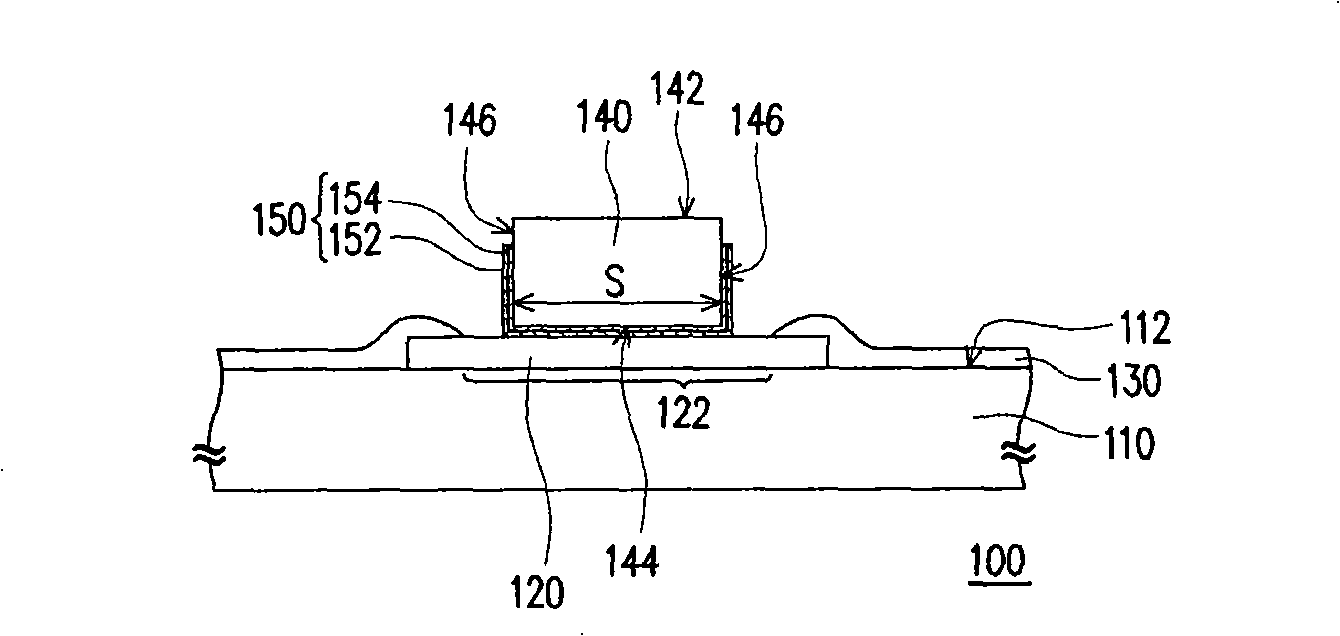
[0042] figure 1 is a schematic cross-sectional view of a semiconductor device according to an embodiment of the present invention. Please refer to figure 1 , the semiconductor device 100 of this embodiment includes a semiconductor substrate 110 , a plurality of pads 120 , a passivation layer 130 , a plurality of bumps 140 and a plurality of seed layers 150 . However, in figure 1 A pad 120 , a bump 140 and a seed layer 150 are represented in the figure. The semiconductor substrate 110 has an active surface 112 . Each pad 120 is disposed on the active surface 112 and is, for example, a metal pad. In the present embodiment, the semiconductor substrate 110 is, for example, a chip, which includes an integrated circuit electrically connected to the pads 120 . The passivation layer 130 is disposed on the active surface 112 and exposes the central portion 122 of each pad 120 . The protective layer is, for example, an insulating layer.

[0043] The seed layer 150 is disposed on ...


PUM


Abstract

The present invention discloses a semiconductor device including a semiconductor substrate, a contact pad, a passivation layer, a bump, and a seeding layer is provided. The semiconductor substrate has an active surface. The contact pad is disposed on the active surface. The passivation layer is disposed on the active surface and exposes a central part of the contact pad. The seeding layer is disposed on the exposed central part of the contact pad. The bump has a top surface, a bottom surface opposite to the top surface, and a side surface connecting the top surface and the bottom surface. The bump is disposed on the seeding layer. The bump is placed in contact with the seeding layer by the bottom surface and by part of the side surface. The present invention also discloses a bump preparing method.

Description

technical field [0001] The invention relates to an electronic device and its technology, and in particular to a semiconductor element and a method for making bumps. Background technique [0002] Flip-chip technology is a packaging technology often used in chip scale packaging (Chip Scale Packaging, CSP). Since the flip-chip technology adopts a planar array (Area Array) for the configuration of the pads on the chip, the packaging area can be reduced. In addition, since the flip-chip technology uses bumps to electrically connect the chip and the carrier, the signal transmission path can be shortened. [0003] Generally, the chip surface is covered with a protective layer, which is present covering the chip surface and exposing the chip's aluminum pads. When the flip-chip technology is in progress, an under bump metal (UBM) layer will be formed on the protection layer and the pads first. Then, a photoresist layer is formed on the UBM layer, but the photoresist layer will exp...

Claims


Application Information

Patent Timeline
Patent Type & Authority Applications(China)
IPC IPC(8): H01L23/485H01L21/60
CPCH01L2224/83851H01L24/83H01L2224/13023H01L2924/01004H01L2224/05624H01L2224/116H01L2224/81903H01L2224/0558H01L2924/01019H01L2224/13144H01L2924/00013H01L2924/01022H01L2224/0401H01L2224/11474H01L2224/1147H01L2224/13016H01L24/11H01L2924/01013H01L2224/11902H01L24/03H01L2924/01047H01L2924/01079H01L24/05H01L2924/14H01L2924/01005H01L2924/01033H01L2924/01006H01L2224/05083H01L2924/01074H01L2924/01078H01L2224/114H01L24/12H01L2224/2929H01L2224/293H01L2924/00011H01L2924/00014H01L2224/13099H01L2224/29075H01L23/488H01K3/22H01L21/44
Inventor 林久顺伍家辉杜文杰
Owner HIMAX TECH LTD
Why Eureka
Try Eureka