Liquid crystal display device and manufacturing method therefor

A technology of a liquid crystal display device and a manufacturing method, which is applied in nonlinear optics, instruments, optics, etc., and can solve the problems of uneven liquid crystal molecular alignment restriction force, reduced light transmittance, and uneven response speed, etc.

Inactive Publication Date: 2012-09-19
SHARP KK
View PDF8 Cites 12 Cited by
  • Summary
  • Abstract
  • Description
  • Claims
  • Application Information

AI Technical Summary

Problems solved by technology

[0005] However, when using slits or ribs, unlike the case where the pretilt direction is defined by the alignment film used in the conventional TN mode, since the slits or ribs are linear, the alignment of liquid crystal molecules is restricted. The force is not uniform within the image elements, so there is a problem with uneven response speed
In addition, the light transmittance decreases in the area where the slit or rib is provided, so there is also a problem that the display brightness decreases

Method used


Image

  • Liquid crystal display device and manufacturing method therefor
  • Liquid crystal display device and manufacturing method therefor
  • Liquid crystal display device and manufacturing method therefor

Examples


Embodiment approach 1

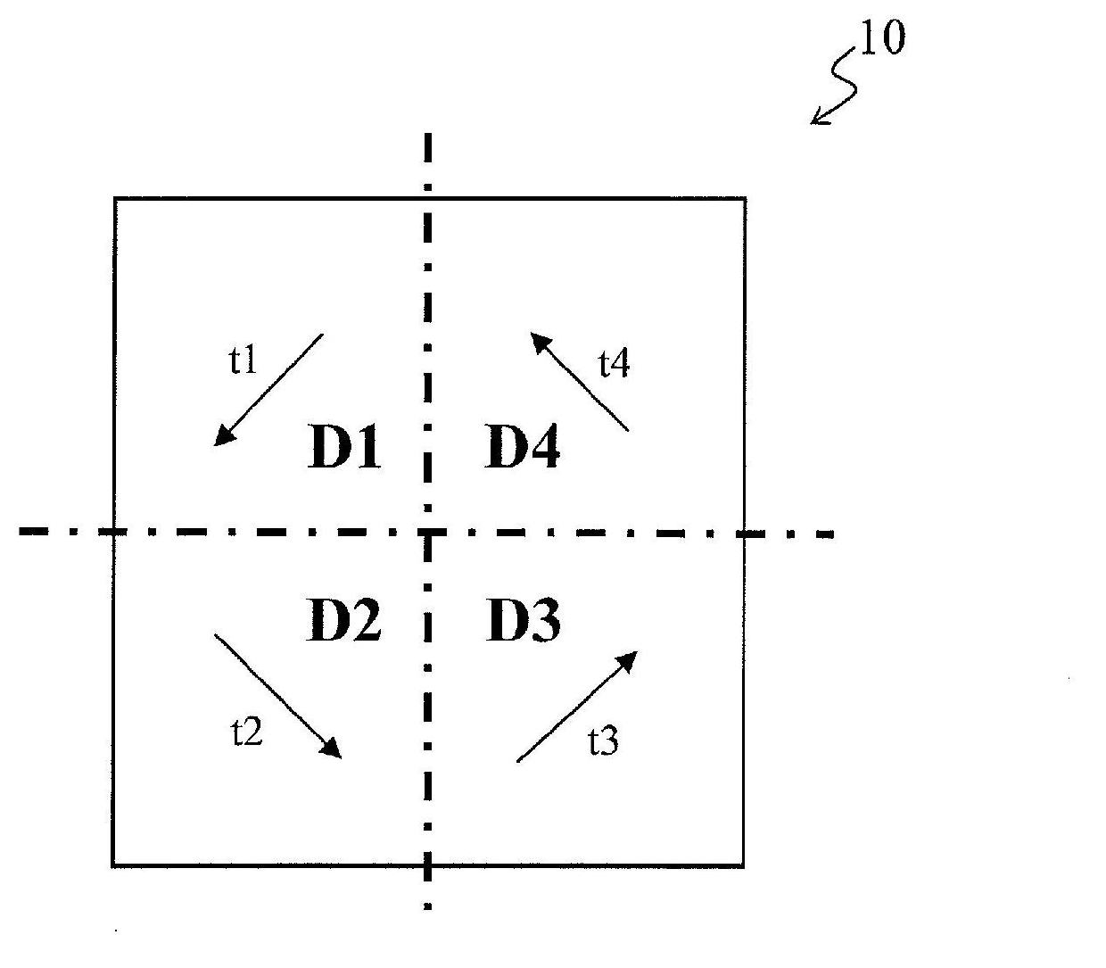
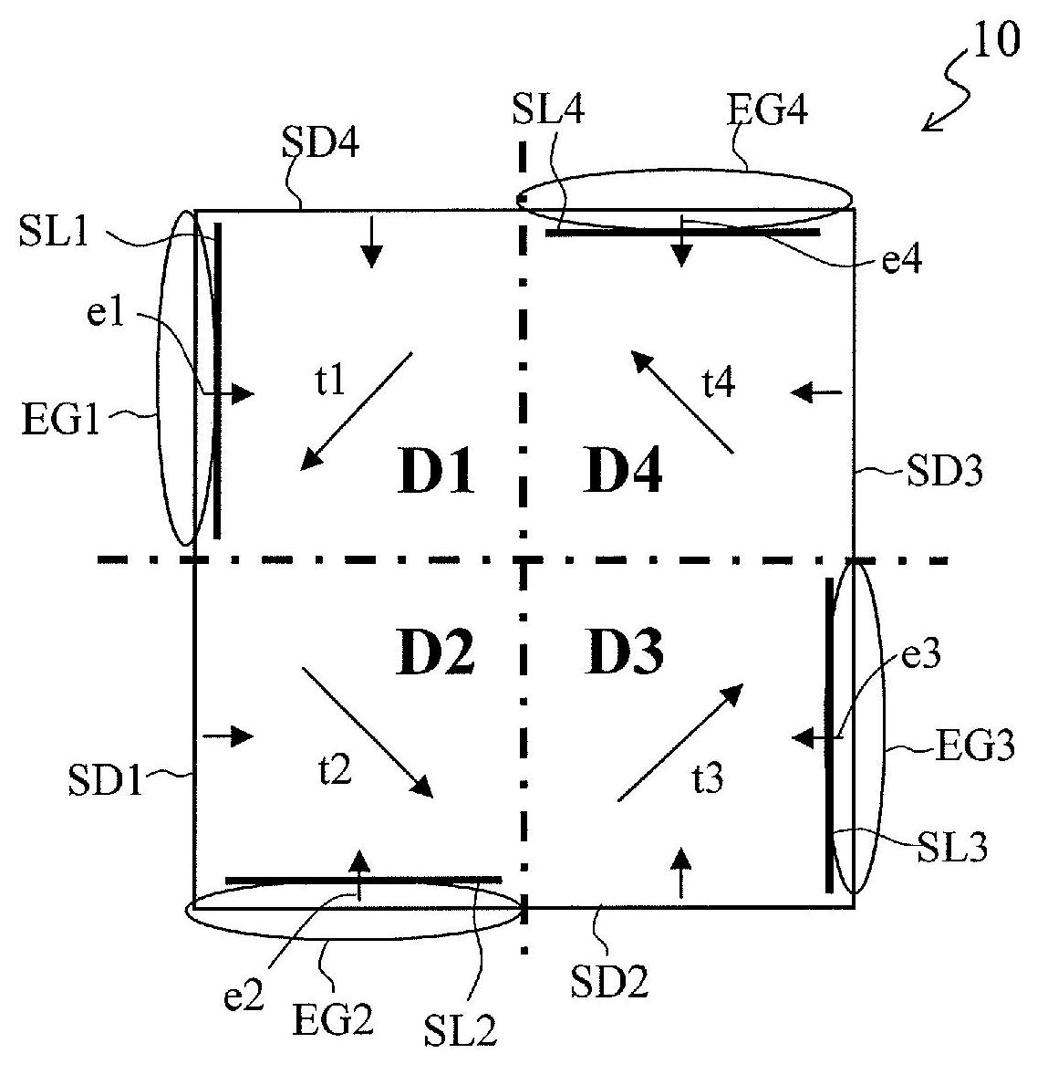
[0162] Before describing the present embodiment, a method for orientationally dividing picture elements in a general 4D-RTN mode and problems in the case of adopting the 4D-RTN mode in a multi-primary-color liquid crystal display device will be described.

[0163] figure 1 Represents a picture element 10 with a 4-segmented orientation structure (4D structure). Also, for simplicity of illustration, figure 1 A substantially square picture element 10 corresponding to a substantially square picture element electrode is shown, but the shape of the picture element is not limited. For example, the image element 10 may be substantially rectangular.

[0164] like figure 1 As shown, the picture element 10 has four liquid crystal domains D1, D2, D3 and D4. exist figure 1 Among them, the areas of the liquid crystal domains D1, D2, D3 and D4 are equal to each other, figure 1 The illustrated example is an example of the most preferable 4D structure in view angle characteristics. ...

Embodiment approach 2

[0275] exist Figure 44 In , the liquid crystal display device 200 in this embodiment is shown. Figure 44 (a) and (b) are plan views schematically showing four pixels P continuous in the row direction of each liquid crystal display device 200 .

[0276] like Figure 44As shown in (a) and (b), it is defined that the lengths of the four picture elements of each pixel P in the row direction are all different. Specifically, the length L1 of the red image element R along the row direction, the length L2 of the blue image element B along the row direction, the length L3 of the yellow image element Y along the row direction, and the length of the green pixel G along the row direction L4 is from large to small in this order (ie L1>L2>L3>L4). In contrast, the lengths in the column direction of all the picture elements are the same length L5. In this way, in the pixel P of the liquid crystal display device 200 of the present embodiment, there is one type of length of picture elemen...

Embodiment approach 3

[0305] Figure 51 The liquid crystal display device 300 in this embodiment is shown. Figure 51 It is a plan view schematically showing six pixels P continuous in the row direction of the liquid crystal display device 300 .

[0306] like Figure 51 As shown in , it is specified that the lengths along the row direction of the four picture elements of each pixel P are all different. Specifically, the length L1 of the red image element R along the row direction, the length L2 of the blue image element B along the row direction, the length L3 of the yellow image element Y along the row direction, and the length of the green pixel G along the row direction L4 is from large to small in this order (ie L1>L2>L3>L4). In contrast, the lengths in the column direction of all the picture elements are the same length L5. In this way, in the pixel P of the liquid crystal display device 300 of the present embodiment, there is one type of length of picture elements in the column direction,...


PUM


Abstract

A liquid crystal display device (100) according to the present invention includes a vertical alignment type liquid crystal layer (3); and a pair of optical alignment films (12, 22). A plurality of picture elements (R, G, B, Y) each include four liquid crystal domains (D1 through D4) in which tilt directions of liquid crystal molecules when a voltage is applied are different. The four liquid crystal domains are located in a matrix of 2 rows 2 columns. The pair of optical alignment films have such an alignment regulation force that causes an identical alignment pattern to appear in repetition in the liquid crystal layer along a first direction which is parallel to one of a row direction and a column direction, with 2n pixels (n is an integer of 1 or greater) being a minimum unit. In the 2n pixels which form the repeat unit of alignment pattern, there are first picture elements and second picture elements in a mixed state, the first picture elements each including the four liquid crystal domains located in a first order, and the second picture elements each including the four liquid crystal domains located in a second order which is different from the first order. According to the present invention, when the 4D-RTN mode is adopted for a liquid crystal display device in which one pixel includes a picture element having a different size from that of another picture element, increase of the cost and the time which are required for optical alignment processing can be suppressed.

Description

technical field [0001] The present invention relates to a liquid crystal display device and a manufacturing method thereof, in particular to a liquid crystal display device with wide viewing angle characteristics and a manufacturing method thereof. Background technique [0002] In recent years, the display characteristics of liquid crystal display devices have been improved, and their use in television receivers and the like has been advancing. Further improvement of viewing angle characteristics of liquid crystal display devices is expected. In particular, there is a strong demand to improve the viewing angle characteristics of a liquid crystal display device (also referred to as a VA-mode liquid crystal display device) using a vertical alignment type liquid crystal layer. [0003] Currently, VA-mode liquid crystal display devices used in large display devices such as televisions employ an alignment division structure in which a plurality of liquid crystal domains are form...

Claims


Application Information

Patent Timeline
Patent Type & Authority Applications(China)
IPC IPC(8): G02F1/1337G02F1/1335G02F1/1343
CPCG02F2001/133742G02F1/133753G02F1/133788G02F2201/52G02F1/133742G02F1/1337G02F1/1335G02F1/1343
Inventor 井上威一郎宫地弘一中川英俊正乐明大
Owner SHARP KK
Why Eureka
Try Eureka