Method of maskless manufacturing of OLED devices

A technology for devices and light-emitting devices, which is applied in the field of maskless manufacturing of OLED devices, can solve the problem of expensive mask processing, and achieve the effects of omitting requirements, small pattern size, and facilitating processing

Inactive Publication Date: 2012-09-26
KONINKLIJKE PHILIPS ELECTRONICS NV
View PDF4 Cites 5 Cited by
  • Summary
  • Abstract
  • Description
  • Claims
  • Application Information

AI Technical Summary

Problems solved by technology

At least, masking in a vacuum is expensive
[0011] Another disadvantage of the masking methods known from the prior art is that, due to the limitations of the shadow mask required, the production of closed non-electrode-coated areas surrounded by coated electrode areas in one coating step is impossible

Method used


Image

  • Method of maskless manufacturing of OLED devices
  • Method of maskless manufacturing of OLED devices
  • Method of maskless manufacturing of OLED devices

Examples


Embodiment Construction

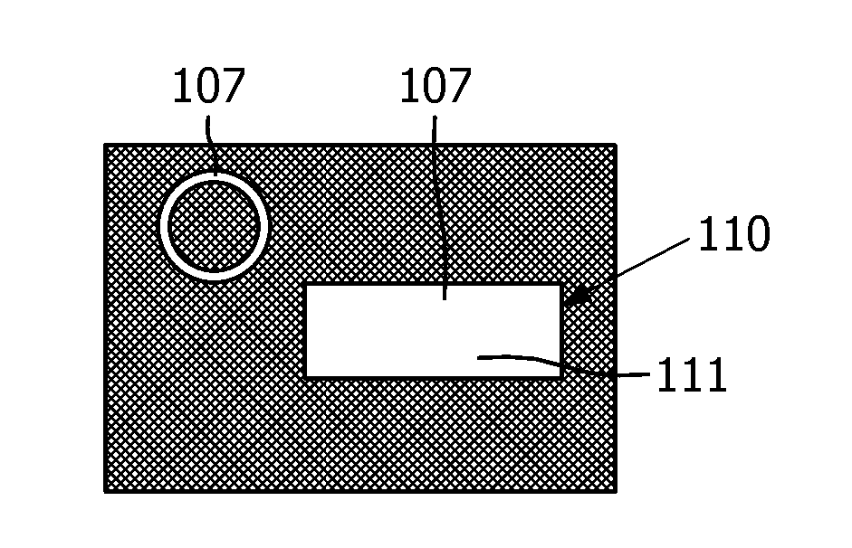
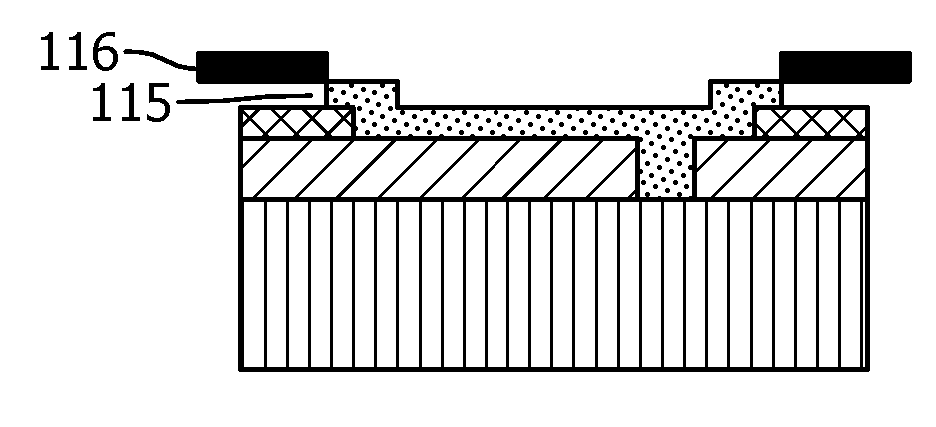
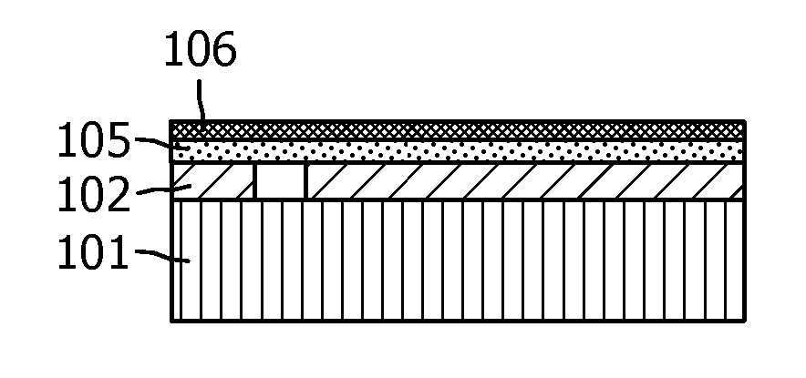
[0062] In FIG. 1 , a process scheme for producing an OLED according to the prior art is shown. In step 1A, a transparent conductor layer 102 is deposited on a carrier substrate 101 in a specific pattern defining the subsequent OLED device structure. Patterning can be done by masking areas not covered by deposition (eg, by sputtering by shadow masking or printing methods). The transparent conductor can be a ZnO, ITO and / or PEDOT / PSS layer. Optional metal lines 113 are deposited on the transparent conductor layer 102 . The patterned structure is filled with optoelectronically active material 105 in step 1B.

[0063] Small molecule optoelectronic active materials are generally deposited by thermal evaporation in vacuum. The deposition of organic material must be limited in such a way that at least the cathode contact 115 is not coated. Usually, the anode contact is also spared from coating, so that a good electrical contact can be obtained later. As can be seen in step 1C, t...


PUM


Abstract

By the invention it is proposed a method of manufacturing of an OLED- device, comprising the steps of providing a carrier substrate, depositing a first electrode material layer on said carrier substrate, forming electrically separated areas within the deposited first electrode material layer, depositing a layer of an organic optoelectronic active material (105) on said first electrode material layer, depositing a second electrode material layer on said organic optoelectronic active material layer.; The method is characterized in that in the steps of depositing the organic optoelectronic active material layer and the second electrode material layer the carrier substrate is covered maskless over its entire functional area with said layers and that at least the second electrode material layer is ablated or rendered non-conductive in at least selected areas to form non-conductive areas within the second electrode material layer.

Description

technical field [0001] The invention relates to the field of manufacturing OLED devices (Organic Light Emitting Diodes). In one aspect, the invention relates to a method of maskless fabrication of an OLED device, in which method the structuring process for forming the OLED device is improved. In another aspect, the invention relates to light emitting devices and systems comprising OLED devices fabricated according to aspects of the invention. Background technique [0002] OLED devices are known from the prior art. Typically, an OLED device consists of at least a first electrode material arranged on a carrier substrate, an organic optoelectronic active material deposited on the first electrode material, and a second electrode material at least partially covering the organic optoelectronic active material. One of the electrode materials acts as the cathode layer, while the other electrode material acts as the anode layer. As the photoelectric active material electroluminesc...

Claims


Application Information

Patent Timeline
Patent Type & Authority Applications(China)
IPC IPC(8): H01L51/00
CPCH01L51/0014H01L51/0023H01L51/5203H10K71/20H10K71/621H10K50/805H10K71/00
Inventor H.施瓦布
Owner KONINKLIJKE PHILIPS ELECTRONICS NV
Why Eureka
Try Eureka