
Semiconductor packaging structure

A semiconductor and structure technology, applied in the field of semiconductor packaging structure, can solve the problems of electromagnetic interference, unstable structure, short service life of several chips, etc., and achieve the effect of prolonging service life, strengthening structure and reducing cost

Active Publication Date: 2012-10-03
ADVANCED SEMICON ENG INC
View PDF4 Cites 20 Cited by
  • Summary
  • Abstract
  • Description
  • Claims
  • Application Information

AI Technical Summary

Problems solved by technology

[0005] In view of this, the object of the present invention is to provide a semiconductor packaging structure to solve the problems of high cost, large volume, unstable structure, short service life, low yield and gap between several chips existing in the existing solder ball technology. Electromagnetic interference and other technical issues

Method used


Image

  • Semiconductor packaging structure
  • Semiconductor packaging structure
  • Semiconductor packaging structure

Examples


Embodiment Construction

[0014] In order to make the above objects, features and advantages of the present invention more comprehensible, preferred embodiments of the present invention are exemplified below and described in detail in conjunction with the accompanying drawings. Furthermore, the directional terms mentioned in the present invention, such as "up", "down", "front", "back", "left", "right", "inside", "outside", "side", etc., It is only for orientation with reference to the attached drawings. Therefore, the directional terms used are used to illustrate and understand the present invention, but not to limit the present invention.

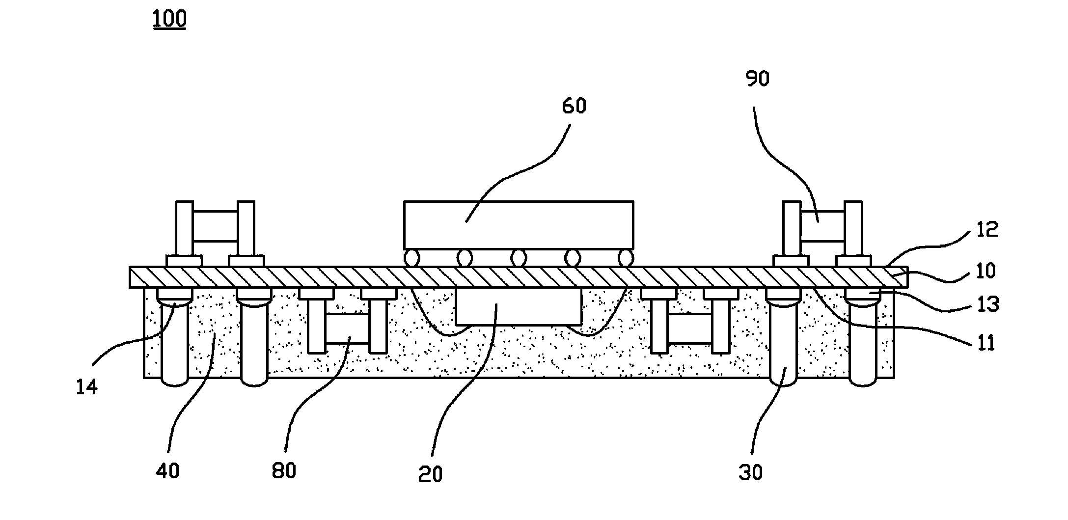
[0015] Please refer to figure 1 As shown, it is a schematic diagram of a semiconductor package structure 100 according to an embodiment of the present invention. The semiconductor package structure 100 of this embodiment mainly includes a substrate 10 , a first chip 20 , several conductive pillars 30 and a sealant layer 40 .

[0016] please refer again figure 1...


PUM

PropertyMeasurementUnit
Heightaaaaaaaaaa
Thicknessaaaaaaaaaa
Thicknessaaaaaaaaaa

Abstract

The invention discloses a semiconductor packaging structure comprising a substrate, a first chip, a plurality of conductive columns, a glue sealing layer and at least one electronic assembly, wherein the substrate is provided with a first surface and a second surface; the first chip is fixedly arranged on the first surface; the conductive columns are electrically connected to the first surface; the glue sealing layer covers the first chip, the first surface and the conductive columns and is exposed out of one end parts of the conductive columns; and at least one electronic assembly is arranged on the second surface of the substrate. The semiconductor packaging structure takes the conductive columns as electrical output terminals, so that the structure is effectively enhanced, the manufacturing yield is improved and the service life is prolonged; and furthermore, the stability of the semiconductor packaging structure is improved.

Description

technical field [0001] The invention relates to a semiconductor packaging structure, in particular to a semiconductor packaging structure that can effectively strengthen the structure, improve the production yield and prolong the service life. Background technique [0002] Nowadays, in order to meet the demands of various high-density packaging, the semiconductor packaging industry gradually develops various types of packaging designs, among which various system in package (SIP) design concepts are often used to structure high-density packaging products. Generally speaking, system packaging can be divided into multi chip module (MCM), package on package (POP) and package in package (PIP). The multi-chip module (MCM) refers to arranging several chips on the same substrate. After the chips are installed, all the chips are embedded with the same encapsulation gel, and can be subdivided into stacked die according to the arrangement of the chips. package or side-by-side package....

Claims


Application Information

Patent Timeline
IPC IPC(8): H01L23/31H01L23/48
CPCH01L2223/6677H01L2224/16H01L2224/16227H01L2224/48227H01L2224/49175H01L2924/15311H01L2924/15321H01L2924/181H01L2924/19105H01L2924/19106H01L2924/00H01L2924/00012
Inventor 廖国宪
Owner ADVANCED SEMICON ENG INC
Learn More