Oxide semiconductor thin film transistor

An oxide semiconductor and thin film transistor technology, applied in transistors, semiconductor devices, electrical components, etc., can solve the problems of increasing the threshold voltage, high carrier concentration, affecting the working stability of oxide semiconductor thin film transistors, etc. achieve high stability

Active Publication Date: 2012-10-10
CHENGDU VISTAR OPTEOLECTRONICS CO LTD
View PDF5 Cites 15 Cited by
  • Summary
  • Abstract
  • Description
  • Claims
  • Application Information

AI Technical Summary

Problems solved by technology

When the thin film transistor is working, the saturation current is determined by the pinch-off of the conduction channel at the drain end, and the carrier concentration is high, which increases the influence on the threshold voltage, which in turn affects the stability of the oxide semiconductor thin film transistor. sex

Method used


Image

  • Oxide semiconductor thin film transistor
  • Oxide semiconductor thin film transistor

Examples


Embodiment 1

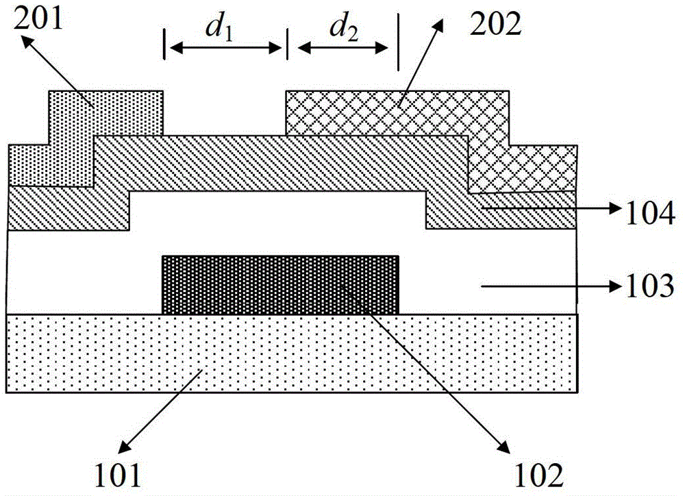
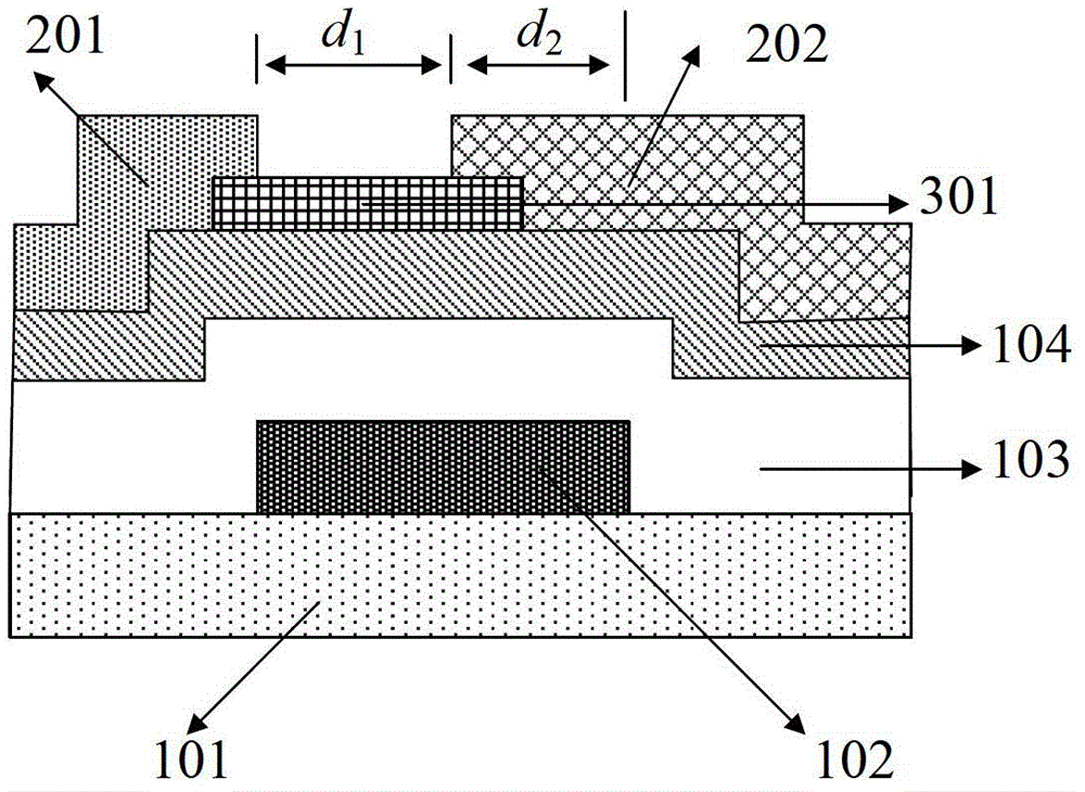
[0035] Such as figure 2 As shown, this embodiment provides an oxide semiconductor thin film transistor, including a substrate 101, a gate electrode 102, an insulating dielectric layer 103, and an oxide semiconductor channel layer 104 sequentially arranged on the substrate 101. The insulating dielectric layer 103 insulates the gate electrode 102 from the oxide semiconductor channel layer 104, the upper surface of the oxide semiconductor channel layer 104 is provided with a drain electrode 201 and a source electrode 202, and the drain electrode 201 and the source electrode The gap between 202 is d 1 , the length of the overlapping region between the source electrode 202 and the gate 102 in the horizontal direction is d 2 The contact between the source electrode 202 and the oxide semiconductor channel layer 104 is a Schottky contact, and the contact between the drain electrode 201 and the oxide semiconductor channel layer 104 is an ohmic contact.

[0036] In order to facilitat...

Embodiment 2

[0050] Such as figure 2 As shown, this embodiment provides an oxide semiconductor thin film transistor, including a substrate 101, a gate electrode 102, an insulating dielectric layer 103, and an oxide semiconductor channel layer 104 sequentially arranged on the substrate 101. The insulating dielectric layer 103 insulates the gate electrode 102 from the oxide semiconductor channel layer 104, the upper surface of the oxide semiconductor channel layer 104 is provided with a drain electrode 201 and a source electrode 202, and the drain electrode 201 and the source electrode The gap between 202 is d 1 , the length of the overlapping region between the source electrode 202 and the gate 102 in the horizontal direction is d 2 The contact between the source electrode 202 and the oxide semiconductor channel layer 104 is a Schottky contact, and the contact between the drain electrode 201 and the oxide semiconductor channel layer 104 is an ohmic contact.

[0051] In order to facilitat...

Embodiment 3

[0065] Such as figure 2 As shown, this embodiment provides an oxide semiconductor thin film transistor, including a substrate 101, a gate electrode 102, an insulating dielectric layer 103, and an oxide semiconductor channel layer 104 sequentially arranged on the substrate 101. The insulating dielectric layer 103 insulates the gate electrode 102 from the oxide semiconductor channel layer 104, the upper surface of the oxide semiconductor channel layer 104 is provided with a drain electrode 201 and a source electrode 202, and the drain electrode 201 and the source electrode The gap between 202 is d 1 , the length of the overlapping region between the source electrode 202 and the gate 102 in the horizontal direction is d 2 The contact between the source electrode 202 and the oxide semiconductor channel layer 104 is a Schottky contact, and the contact between the drain electrode 201 and the oxide semiconductor channel layer 104 is an ohmic contact.

[0066]In order to facilitate...


PUM


Abstract

The invention provides an oxide semiconductor thin film transistor which comprises a substrate, a gate electrode, an insulation dielectric layer and an oxide semiconductor channel layer, wherein the gate electrode, the insulation dielectric layer and the oxide semiconductor channel layer are sequentially arranged on the substrate, the insulation dielectric layer enables the gate electrode and the oxide semiconductor channel layer to be insulted, a drain electrode and a source electrode are arranged on the upper surface of the oxide semiconductor channel layer, a gap between the drain electrode and the source electrode is d1, the length of an overlapping region of the source electrode and the gate electrode in the horizontal direction is d2, contact between the source electrode and the oxide semiconductor channel layer is schottky contact, and the contact between the drain electrode and the oxide semiconductor channel layer is ohmic contact. The short-channel effect on the oxide semiconductor thin film transistor is small due to new geometrical characteristics and operating principles, and the oxide semiconductor thin film transistor is favorable for improvement of consistency.

Description

technical field [0001] The invention relates to an oxide semiconductor thin film transistor, which belongs to the field of flat panel display. Background technique [0002] Thin-film transistors (TFTs), as active drive devices for flat-panel displays, have become key technologies in the field of flat-panel displays. Oxide semiconductor (such as IGZO, AZO, GZO, ZnO, etc.) thin film transistors have good development prospects due to their high transparency, high mobility, high current switching ratio, low process temperature, and simple manufacturing process. Used on high-performance TFT-LCD or AMOLED displays. [0003] However, the threshold voltage of the current oxide semiconductor thin film transistors tends to drift over time during operation (such as in constant voltage or constant current mode), which affects the stability of the threshold voltage and thus affects the brightness of display pixels. adverse effects. [0004] Studies have found that the concentration of...

Claims


Application Information

Patent Timeline
Patent Type & Authority Applications(China)
IPC IPC(8): H01L29/786H01L29/45H01L29/47
Inventor 陈红邱勇黄秀颀魏朝刚
Owner CHENGDU VISTAR OPTEOLECTRONICS CO LTD
Why Eureka
Try Eureka