Charge pump based on voltage multiplier cascade connection
A technology of voltage doubler and charge pump, which is applied in the field of DC-DC boosting to achieve high practical value, precise erasing operation, and cost reduction
- Summary
- Abstract
- Description
- Claims
- Application Information
AI Technical Summary
Problems solved by technology
Method used
Image
Examples
Embodiment 1
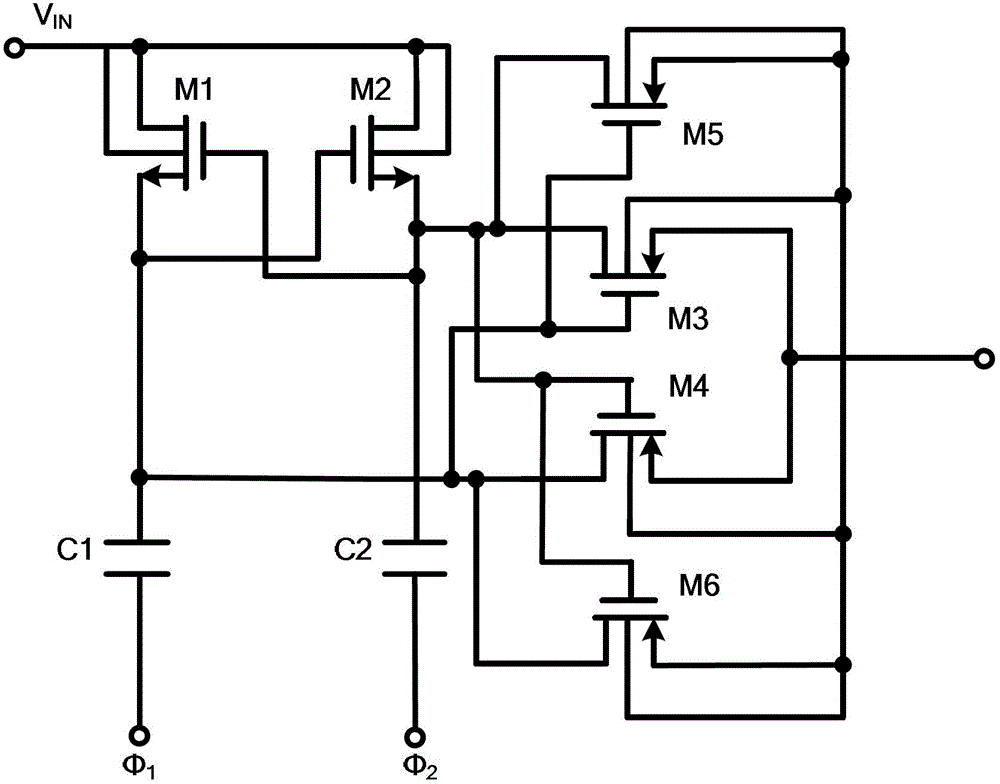
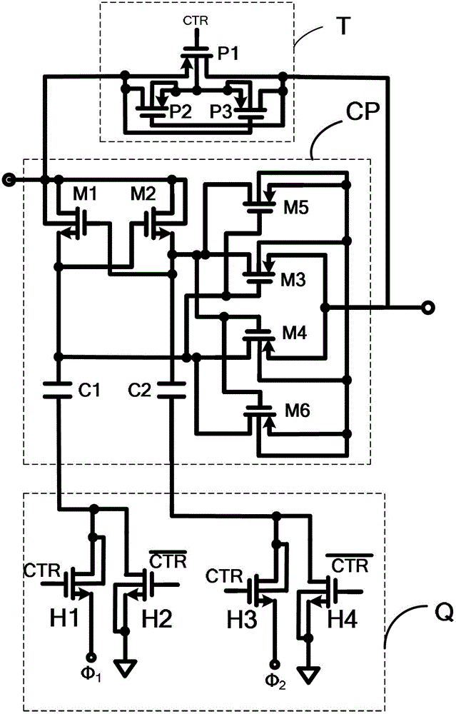
[0042] Such as Figure 4 As shown, a charge pump based on voltage doubler cascade is formed by cascading N voltage doubler units, and the voltage doubler unit receives a pair of phase-complementary clock signals Φ1~Φ2 provided by external equipment; The voltage doubler units all use voltage doubler circuits, and the rest of the voltage doubler units use voltage doublers. The input end of the first stage voltage doubler unit receives the input voltage V provided by external equipment. IN , the output terminal of the last stage voltage doubler unit generates the output voltage V OUT ; Both N and K are natural numbers greater than 0, and 1≤K≤N;
[0043] In this embodiment, the rated input voltage range is 1.5V-2.1V, and the rated output voltage is 6.75V. The input voltage and output voltage satisfy the following relationship:
[0044] V IN = V OUT N ...
Embodiment 2
[0063] Such as Image 6 As shown, a charge pump based on cascaded voltage doubler, the rated input voltage range is 1.5V ~ 2.1V, and the specified required output voltage is 6.75V; therefore, it is composed of five voltage doubler units cascaded, and the voltage doubler The unit receives a pair of phase-complementary clock signals Φ1~Φ2 provided by external equipment; among them, the first three-stage voltage doubler units all use voltage doubler circuits, the last two-stage voltage doubler units all use voltage doublers, and the first-stage voltage doubler units use voltage doublers. The input terminal receives the input voltage V provided by the external device IN , the output terminal of the last stage voltage doubler unit generates the output voltage V OUT ; The first clock terminal and the second clock terminal of the voltage doubler circuit adopted by the first three stages of voltage doubler units respectively receive clock signals Φ1-Φ2.
[0064] Such as Figure 5 A...
PUM
 Abstract
Description
Claims
Application Information


