Manufacturing method for circuit board

A production method and circuit board technology, which are applied in the reinforcement of conductive patterns, secondary processing of printed circuits, etc., can solve problems such as short circuit of circuit board products, and achieve the effects of avoiding gold long corners, avoiding side erosion, and improving production yield.

Inactive Publication Date: 2012-10-10
AVARY HLDG (SHENZHEN) CO LTD +1
View PDF4 Cites 7 Cited by
  • Summary
  • Abstract
  • Description
  • Claims
  • Application Information

AI Technical Summary

Problems solved by technology

Such excess gold is easy to conduct with the conductive lines covered by the solder mask, thus causing a short circuit of the circuit board product

Method used


Image

  • Manufacturing method for circuit board
  • Manufacturing method for circuit board
  • Manufacturing method for circuit board

Examples


Embodiment Construction

[0021] The manufacturing method of the circuit board provided by the first embodiment of the technical solution includes the following steps:

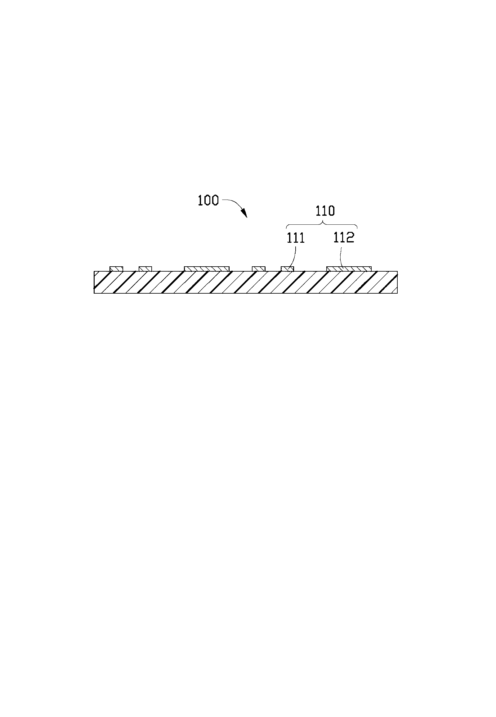
[0022] For a first step, see figure 1 , providing a substrate 100 .

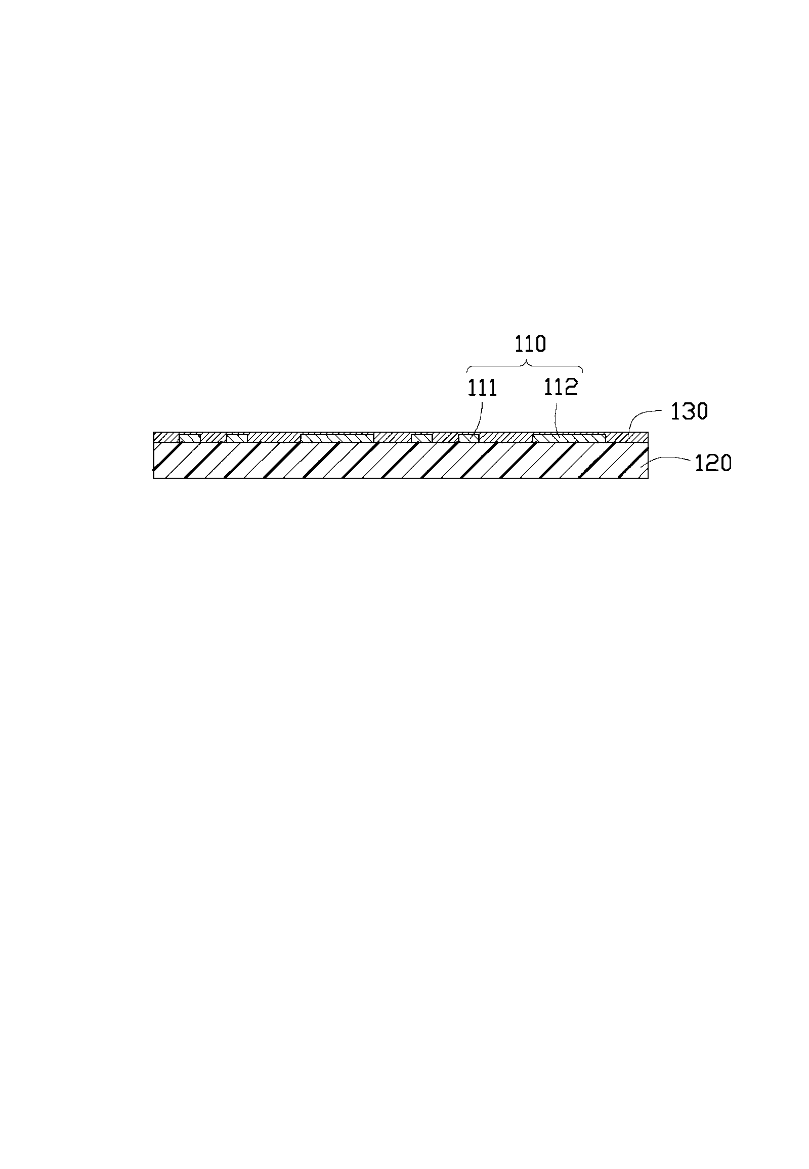
[0023] The substrate 100 includes a substrate layer 120 and a circuit pattern 110 formed on the substrate layer 120 . The circuit pattern 110 includes a plurality of conductive circuits 111 and a plurality of pads 112 for electrically communicating with the outside world. Each pad 112 is in electrical communication with one or more conductive lines 111 . The substrate 100 may be a single-sided circuit board, or a double-sided circuit board or a multi-layer circuit board, that is, the substrate layer 120 may be an insulating layer, or may include alternately arranged conductive layers and insulating layers. In this embodiment, the substrate 100 is a single-sided circuit board, and the base material layer 120 is an insulating layer.

[0024] It can be understood th...


PUM


Abstract

A manufacturing method for a circuit board comprises steps of: providing a substrate with a line pattern which comprises a plurality of bonding pads; forming a first ink layer with thickness of 0.2 mil to 1.0 mil on the surface of the line pattern; printing black ink on the first ink layer and forming a second ink layer with thickness of 0.2 mil to 1.0 mil; forming an ink lamination structure composed of the first ink layer and the second ink layer and baking the ink lamination structure; removing a part of ink lamination structure through exposure and development, forming a plurality of openings and exposing each bonding pad from one of the opening; and forming gold layers on the surface of the plurality of bonding pads which are exposed from the plurality of openings. The technical scheme provided by the manufacturing method for the circuit board can effectively prevent a phenomenon of gold redundancy.

Description

technical field [0001] The invention relates to the field of manufacturing printed circuit boards, in particular to a method for manufacturing a circuit board. Background technique [0002] Printed circuit boards have been widely used due to their advantages such as high assembly density. For the application of the circuit board, please refer to the literature Takahashi, A. Ooki, N. Nagai, A. Akahoshi, H. Mukoh, A. Wajima, M. Res. Lab, High density multilayer printed circuit board for HITAC M-880, IEEE Trans . on Components, Packaging, and Manufacturing Technology, 1992, 15(4): 418-425. [0003] In the production process of the printed circuit board, it is necessary to form a solder resist layer on the outer surface of the printed circuit board. The solder resist layer will cover the part of the outer layer to the electric circuit that does not need to communicate with the outside world, and will cover the part that needs to communicate with the outside world. Part of the ...

Claims


Application Information

Patent Timeline
Patent Type & Authority Applications(China)
IPC IPC(8): H05K3/24
Inventor 蔡宗青柳超陈柏同
Owner AVARY HLDG (SHENZHEN) CO LTD
Why Eureka
Try Eureka