Packaging structure of integrated magnetic and accelerometer and packaging method thereof
A technology of acceleration sensor and magnetic sensor, which is applied in the direction of electric solid-state devices, semiconductor devices, semiconductor/solid-state device components, etc., can solve the problems of increasing product cost, wasting PCB board space, reducing product assembly efficiency, etc., and achieving packaging cost , expand the effect of the application
- Summary
- Abstract
- Description
- Claims
- Application Information
AI Technical Summary
Problems solved by technology
Method used
Image
Examples
no. 1 example 100
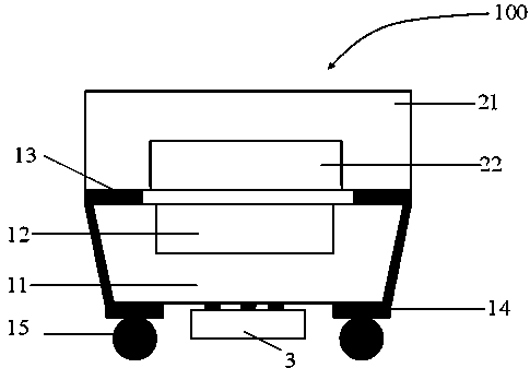
[0034] See figure 1 As shown, the present invention relates to a first embodiment 100 of a packaging structure integrating magnetic and acceleration sensors, which includes a first wafer 11 and a second wafer 21 .
[0035] Wherein the first wafer 11 is provided with a driving circuit for driving the acceleration sensor and a magnetic sensor and a structural circuit (not shown) of the acceleration sensor, and a first cavity 12 is also provided on the first wafer 11, and in the first cavity 12 A mechanical structure with an acceleration sensor. In addition, the front side of the first wafer 11 is provided with metal pads 13 outside the first cavity 12 .
[0036] The second wafer 21 is bonded on top of the first wafer 11 . A second cavity 22 for matching with the first cavity 12 is opened thereon, and the width of the second cavity 22 along the surface of the wafer is greater than or equal to the size of the mechanical mechanism of the acceleration sensor.
[0037] Metal wires...
no. 2 example 200
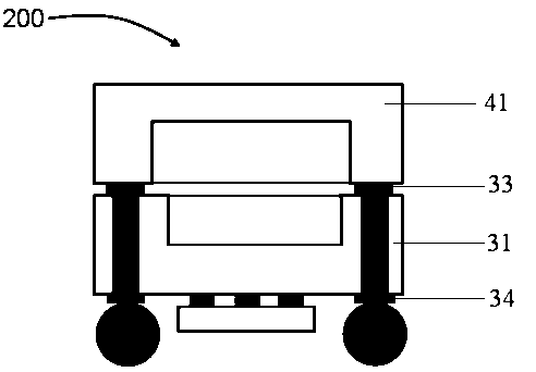
[0038] Further, such as figure 2 As shown, it illustrates the second embodiment 200 of the packaging structure of the integrated magnetic and acceleration sensor involved in the present invention, its structure is similar to that of the first embodiment, and also includes a first wafer 31 and a second wafer 41 . The difference between it and the first embodiment lies in the way in which the metal wire 34 is drawn out from the metal pad (pad) 33, which is to drill a hole on the first wafer 31 and lead out through the through-silicon via (TSV) process. The lead-out of the pad in the first embodiment is realized through a sidewall lead process.
[0039] Further, such as image 3 -6, the present invention also provides a packaging method for manufacturing the packaging structure of the integrated magnetic and acceleration sensor involved in the present invention, which includes the following steps:
[0040] 1. First wafer and second wafer preparation and processing (such as ...
PUM
 Abstract
Description
Claims
Application Information


