Preparation method of gate oxide integrity (GOI) wafer structure

A wafer and stacked structure technology, which is applied in semiconductor/solid-state device manufacturing, electrical components, circuits, etc., can solve the problems of high dislocation density and complex process of GOI wafers, and achieve improved germanium concentration technology, simple process, and reduced penetration effect of dislocation

Active Publication Date: 2012-10-17
SHANGHAI INST OF MICROSYSTEM & INFORMATION TECH CHINESE ACAD OF SCI
View PDF6 Cites 11 Cited by
  • Summary
  • Abstract
  • Description
  • Claims
  • Application Information

AI Technical Summary

Problems solved by technology

[0005] In view of the shortcomings of the prior art described above, the object of the present invention is to provide a method for prepari...

Method used


Image

  • Preparation method of gate oxide integrity (GOI) wafer structure
  • Preparation method of gate oxide integrity (GOI) wafer structure
  • Preparation method of gate oxide integrity (GOI) wafer structure

Examples


Embodiment Construction

[0042] Embodiments of the present invention are described below through specific examples, and those skilled in the art can easily understand other advantages and effects of the present invention from the content disclosed in this specification. The present invention can also be implemented or applied through other different specific implementation modes, and various modifications or changes can be made to the details in this specification based on different viewpoints and applications without departing from the spirit of the present invention.

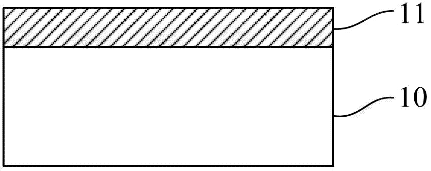
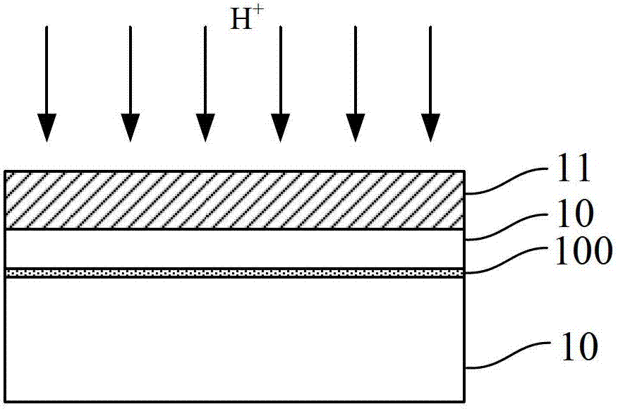
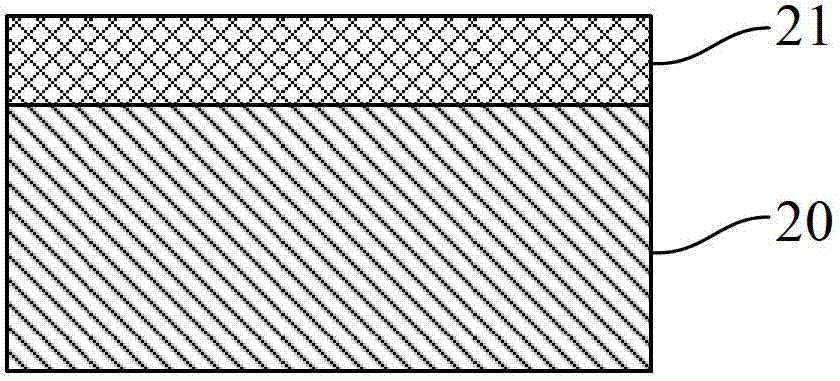
[0043] see Figure 1a to Figure 1f ,as well as Figure 2 to Figure 3 . It should be noted that the diagrams provided in this embodiment are only schematically illustrating the basic idea of ​​the present invention, and only the components related to the present invention are shown in the diagrams rather than the number, shape and shape of the components in actual implementation. Dimensional drawing, the type, quantity and proportion...


PUM

PropertyMeasurementUnit
Thicknessaaaaaaaaaa
Thicknessaaaaaaaaaa
Thicknessaaaaaaaaaa

Abstract

The invention provides a preparation method of a gate oxide integrity (GOI) wafer structure, which comprises the following steps that firstly, a SiGe-on-insulator (SGOI) wafer structure is prepared through a Smart-Cut technology, then germanium concentration is carried out on the SGOI wafer structure, and the GOI wafer structure is obtained. Because the SGOI which is prepared through the Smart-Cut technology basically is not mismatched or dislocated on an SGOI/BOX interface, the penetrated dislocation of the GOI is finally reduced. According to the preparation method of the GOI wafer structure, the process is simple, the high-quality GOI wafer structure can be realized, a germanium concentration technology is greatly improved, an ion injection technology and an annealing technology are very mature processes in the current semi-conductor industry, and the preparation method greatly improves the wide application possibility of germanium concentration in the semi-conductor industry.

Description

technical field [0001] The invention relates to a method for preparing a wafer structure, in particular to a method for preparing a GOI wafer structure. Background technique [0002] With the rapid development of silicon-based large-scale integrated circuit technology, the performance of bulk silicon CMOS devices has gradually approached the physical limit of silicon materials, and further improving the performance of bulk silicon CMOS devices in the direction guided by Moore's law will face increasing investment and market risk. The semiconductor industry is a market that is very sensitive to the performance-price ratio of products. How to continuously improve the performance of silicon-based devices based on the existing VLSL process without increasing investment has become a common problem in the industry. The exploration of new materials and new processes is undoubtedly an important way of thinking and research direction to solve this problem. [0003] Germanium-on-in...

Claims


Application Information

Patent Timeline
IPC IPC(8): H01L21/762
CPCH01L21/20H01L21/76254
Inventor 张苗叶林狄增峰薛忠营
Owner SHANGHAI INST OF MICROSYSTEM & INFORMATION TECH CHINESE ACAD OF SCI
Why Eureka
Try Eureka