Monolithic heterogeneous integrated structure of silicon on insulating substrate and III-V device and preparation method of monolithic heterogeneous integrated structure

A III-V technology on an insulating substrate, applied in semiconductor/solid-state device manufacturing, semiconductor devices, electrical components, etc., can solve problems such as difficulty in ensuring material uniformity and yield, and reduce the probability of threading dislocations. Wide application value, reduce the effect of leakage channel

Pending Publication Date: 2022-08-09
浙江集迈科微电子有限公司
View PDF0 Cites 0 Cited by
  • Summary
  • Abstract
  • Description
  • Claims
  • Application Information

AI Technical Summary

Problems solved by technology

[0006] In view of the shortcomings of the prior art described above, the object of the present invention is to provide a monolithic heterogeneous integration structure of silicon on an insulating substrate and III-V group devices and its preparation method, which is used to solve the problem of GaN devices in the prior art. It is difficult to ensure the uniformity and yield of materials in heterogeneous integrated structures with Si devices and / or III-V devices

Method used


Image

  • Monolithic heterogeneous integrated structure of silicon on insulating substrate and III-V device and preparation method of monolithic heterogeneous integrated structure
  • Monolithic heterogeneous integrated structure of silicon on insulating substrate and III-V device and preparation method of monolithic heterogeneous integrated structure
  • Monolithic heterogeneous integrated structure of silicon on insulating substrate and III-V device and preparation method of monolithic heterogeneous integrated structure

Examples


Embodiment Construction

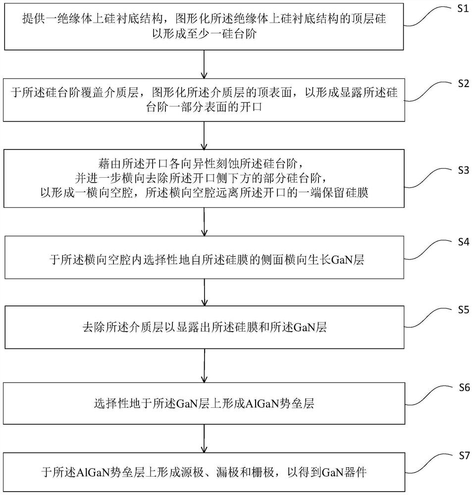
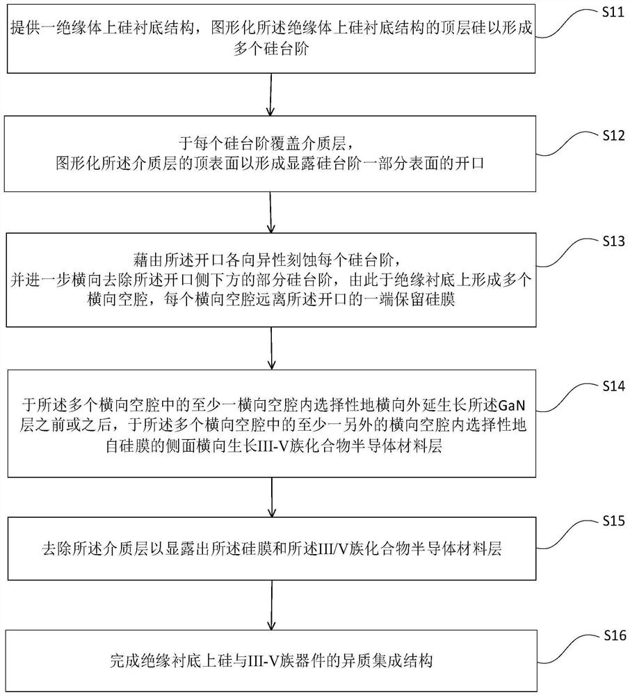
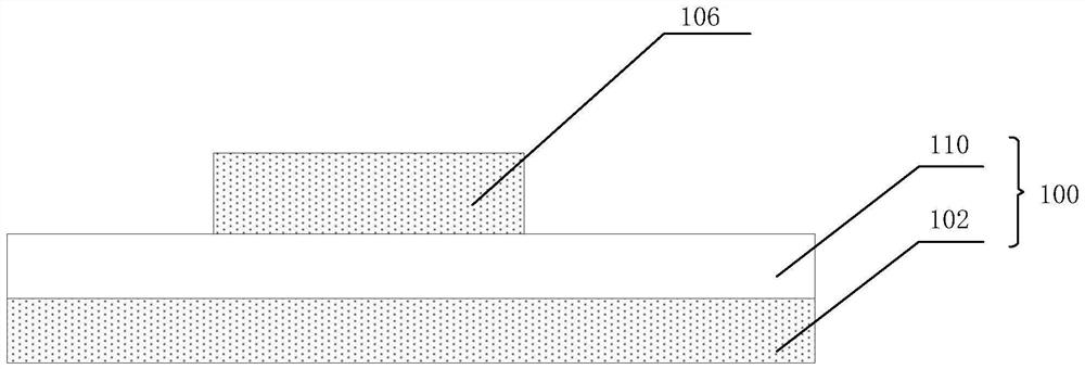
[0051] The embodiments of the present invention are described below through specific specific examples, and those skilled in the art can easily understand other advantages and effects of the present invention from the contents disclosed in this specification. The present invention can also be implemented or applied through other different specific embodiments, and various details in this specification can also be modified or changed based on different viewpoints and applications without departing from the spirit of the present invention.

[0052] When describing the embodiments of the present invention in detail, for the convenience of explanation, the cross-sectional views showing the device structure will not be partially enlarged according to the general scale, and the schematic diagrams are only examples, which should not limit the protection scope of the present invention. In addition, the three-dimensional spatial dimensions of length, width and depth should be included i...


PUM


Abstract

According to the monolithic heterogeneous integrated structure of the silicon on the insulating substrate and the III-V device and the preparation method of the monolithic heterogeneous integrated structure, the Si-based insulating substrate can be adopted for heterogeneous integration in the preparation method, and the Si substrate has price and cost advantages; the GaN layer is transversely grown from the side surface of the silicon film, and stress accumulation caused by lattice mismatch and thermal mismatch between the GaN epitaxial layer and the substrate can be reduced by reducing the contact area of the growth substrate and the GaN layer, so that the probability of penetration dislocation is reduced, and the high-quality epitaxial layer can be obtained. The monolithic heterogeneous integrated structure of the silicon on the insulating substrate and the III-V device, which is obtained based on the preparation method, can be used for preparing a cascode cascade type GaN-based device, and is beneficial to miniaturization of the device and development of the advantages of the GaN cascode device in the aspects of power gain and stability.

Description

technical field [0001] The invention belongs to the technical field of semiconductors, and relates to a monolithic hetero-integrated structure of silicon and III-V group devices and a preparation method. Background technique [0002] With the development of semiconductor technology, more and more attention has been paid to miniaturized and higher integrated chips. Among them, various functional devices are integrated on a single chip to make the entire package module smaller, higher performance, and economical. The cost of the back-end process is getting more and more attention. [0003] As a representative of the third generation semiconductor materials, gallium nitride (GaN) has many excellent properties such as high critical breakdown electric field, high electron mobility, high two-dimensional electron gas concentration and good high temperature working ability. Therefore, based on GaN The third generation of semiconductor devices, such as high electron mobility transis...

Claims


Application Information

Patent Timeline
Patent Type & Authority Applications(China)
IPC IPC(8): H01L21/335H01L29/778
CPCH01L29/66462H01L29/7783
Inventor 蔡泉福严鹏陈哲余松波吴蒙
Owner 浙江集迈科微电子有限公司
Why Eureka
Try Eureka