Semiconductor device possessing memristor characteristic and method for realizing multilevel storage

A multi-level storage and semiconductor technology, which is applied in semiconductor devices, electric solid-state devices, information storage, etc., can solve the problems of reducing device area and storage capacity, and achieve the effect of increasing storage capacity and reducing production costs

Inactive Publication Date: 2012-10-17
INST OF MICROELECTRONICS CHINESE ACAD OF SCI
View PDF3 Cites 13 Cited by
  • Summary
  • Abstract
  • Description
  • Claims
  • Application Information

AI Technical Summary

Problems solved by technology

Therefore, it is difficult to increase the storage capacity simply by reducing the device area.

Method used


Image

  • Semiconductor device possessing memristor characteristic and method for realizing multilevel storage
  • Semiconductor device possessing memristor characteristic and method for realizing multilevel storage
  • Semiconductor device possessing memristor characteristic and method for realizing multilevel storage

Examples


Embodiment Construction

[0022] In order to make the object, technical solution and advantages of the present invention clearer, the present invention will be described in further detail below in conjunction with specific embodiments and with reference to the accompanying drawings. The drawings and their descriptions provided herein are only for illustrating embodiments of the present invention. The shapes and dimensions in the respective drawings are for schematic illustration only, and do not strictly reflect actual shapes and dimensional ratios. In the illustrations of the embodiments of the present invention, they are all represented by rectangles, and the representations in the figures are schematic and not intended to limit the scope of the present invention.

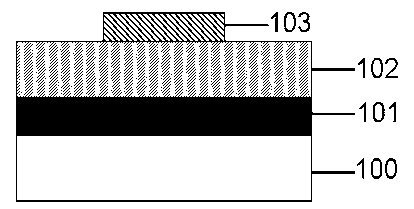
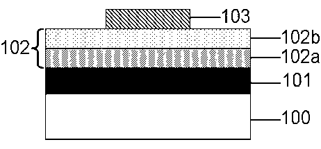
[0023] figure 1 It is a schematic structural diagram of a semiconductor device with memristor characteristics according to an embodiment of the present invention. Such as figure 1 As shown, in this embodiment, a semiconductor device wi...


PUM


Abstract

The invention relates to a semiconductor device possessing a memristor characteristic and a method for realizing multilevel storage. The semiconductor device comprises an upper electrode, a lower electrode and a storage medium layer arranged between the upper electrode and the lower electrode. According to the invention, when the semiconductor device possessing the memristor characteristic generates mutual conversion between a high impedance state and a low impedance state, different high impedance state or low impedance state resistance values can be obtained through controlling a conversion voltage so that multilevel storage of multi-bit data is stored in each memory cell; a storage capacity of the semiconductor device possessing the memristor characteristic is increased and making cost of the semiconductor device possessing the memristor characteristic is reduced.

Description

technical field [0001] The invention relates to a semiconductor device and a method for realizing multi-level storage thereof, in particular to a semiconductor device with memristor characteristics and a method for realizing multi-level storage thereof, belonging to the field of microelectronic technology and memory devices. Background technique [0002] Semiconductor memory plays a very important role in the field of microelectronics technology. Memory can generally be divided into two types: volatile and non-volatile. Compared with volatile memory, the biggest advantage of non-volatile memory is that the stored data can be kept for a long time without power supply, so it has become a widely used and generally recognized memory type. With the increasing popularity of portable personal devices such as mobile phones, MP4 and notebook computers, and the need for large-capacity and low-power storage in multimedia applications and mobile communications, non-volatile memory pla...

Claims


Application Information

Patent Timeline
Patent Type & Authority Applications(China)
IPC IPC(8): H01L45/00H01L27/24G11C11/56
Inventor 刘明李颖弢龙世兵刘琦吕杭炳
Owner INST OF MICROELECTRONICS CHINESE ACAD OF SCI
Why Eureka
Try Eureka