Bulk acoustic wave resonator and method of manufacturing thereof

A resonator, bulk acoustic wave technology, applied in resonators, waveguide devices, impedance networks, etc., to avoid measurement and simplify driving integrated circuits

Inactive Publication Date: 2012-10-17
VTT科技研究中心 +1
View PDF3 Cites 1 Cited by
  • Summary
  • Abstract
  • Description
  • Claims
  • Application Information

AI Technical Summary

Problems solved by technology

Therefore, it is difficult or impossible to apply them to mass production

Method used


Image

  • Bulk acoustic wave resonator and method of manufacturing thereof
  • Bulk acoustic wave resonator and method of manufacturing thereof
  • Bulk acoustic wave resonator and method of manufacturing thereof

Examples


example 1

[0074] Example 1: SE plate oriented along crystallographic direction, circular void

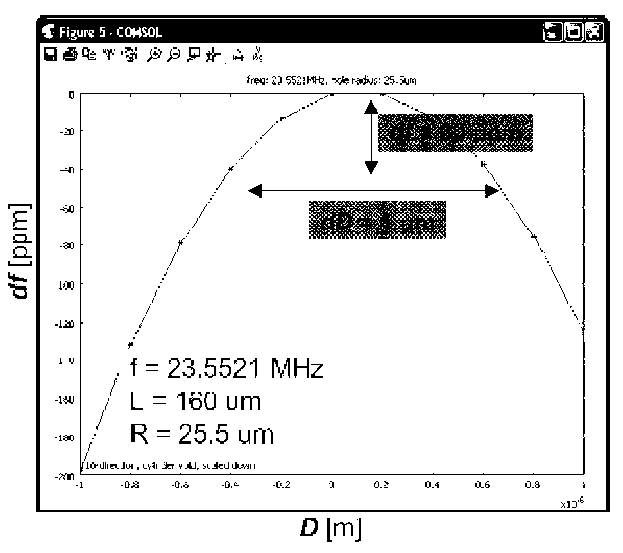
[0075] A single crystal silicon plate resonator operating in SE mode is analyzed. The side edges of the plate are aligned along the crystal direction and have a side length of L=320 μm. The optimal circular void radius is 38 μm ( Figure 6a ). Figure 6b The frequency variation of a similar resonator reduced in size by a factor of two is shown.

example 2

[0076] Example 2: SE plate oriented along the crystallographic direction, circular void. exist Figure 7a with Figure 7b shown in the Figure 6a with Figure 6bCorresponding results (plate size 320 μm and 160 μm).

example 3

[0077] Example 3: SE plate oriented along the crystallographic direction, with rectangular voids. exist Figure 8 The results for a plate size of 320 μm are shown in .


PUM


Abstract

The invention concerns a novel bulk acoustic wave (BAW) resonator design and method of manufacturing thereof. The bulk acoustic wave resonator comprises a resonator portion, which is provided with at least one void having the form of a trench which forms a continuous closed path on the resonator portion. By manufacturing the void in the same processing step as the outer dimensions of the resonator portion, the effect of processing variations on the resonant frequency of the resonator can be reduced. By means of the invention, the accuracy of BAW resonators can be increased.

Description

technical field [0001] This invention relates to micromechanical resonators, and more particularly to bulk acoustic wave (BAW) resonators and the like. Background technique [0002] The frequency of a lateral bulk acoustic wave mode MEMS resonator, such as a plate resonator, is defined by the lateral dimension(s) of the device. f=v / (2L) The frequencies of a plate resonator operating in its square extensional (SE, square extensional) mode are given with good precision, where v is the sound velocity and L is the length of the plate side, respectively. Due to manufacturing process imperfections, the resonator dimensions vary within the wafer and from wafer to wafer, which leads to variations in the resonant frequency of the manufactured device. [0003] The lateral dimensions of the resonator are typically defined by the etched trenches created using, for example, deep reactive ion etching (DRIE) process steps ( Figure 1a shown in ) to limit. Typical variations in L can exc...

Claims


Application Information

Patent Timeline
Patent Type & Authority Applications(China)
IPC IPC(8): H03H9/02H03H9/15H03H3/04H03H3/007H01P7/06
CPCH03H2009/0233H03H9/2436H01P7/082H03H3/0076H01P11/008H03H2009/241H03H9/172H03H2009/2442H01P7/06H03H3/02H03H9/15
Inventor A.贾科拉H.库伊斯马
Owner VTT科技研究中心
Why Eureka
Try Eureka