Optical on-chip network system of non-blocking communication and communication method thereof

An optical on-chip network, non-blocking technology, applied in the field of communications, can solve the problems of increasing chip area and layout complexity, unable to truly achieve non-blocking communication, low resource utilization, etc., to improve resource utilization and throughput performance, The effect of simplifying design and reducing communication delay

Inactive Publication Date: 2012-11-14
XIDIAN UNIV
View PDF6 Cites 13 Cited by
  • Summary
  • Abstract
  • Description
  • Claims
  • Application Information

AI Technical Summary

Problems solved by technology

Too many waveguides also increases chip area and layout complexity
[0006] Although the above two methods can reduce the probability of blocking, they cannot truly achieve non-blocking communication; at the same time, the resource utilization rate of these two methods is low, and the throughput performance is poor.

Method used


Image

  • Optical on-chip network system of non-blocking communication and communication method thereof
  • Optical on-chip network system of non-blocking communication and communication method thereof
  • Optical on-chip network system of non-blocking communication and communication method thereof

Examples


Embodiment Construction

[0032] In order to more clearly introduce the optical network-on-chip system for non-blocking communication proposed by the present invention, the following will describe in detail with reference to the accompanying drawings and specific examples.

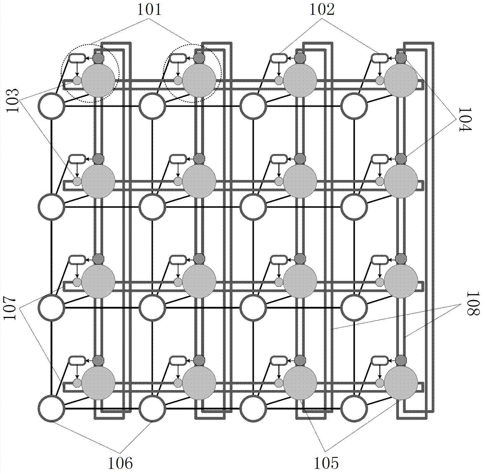
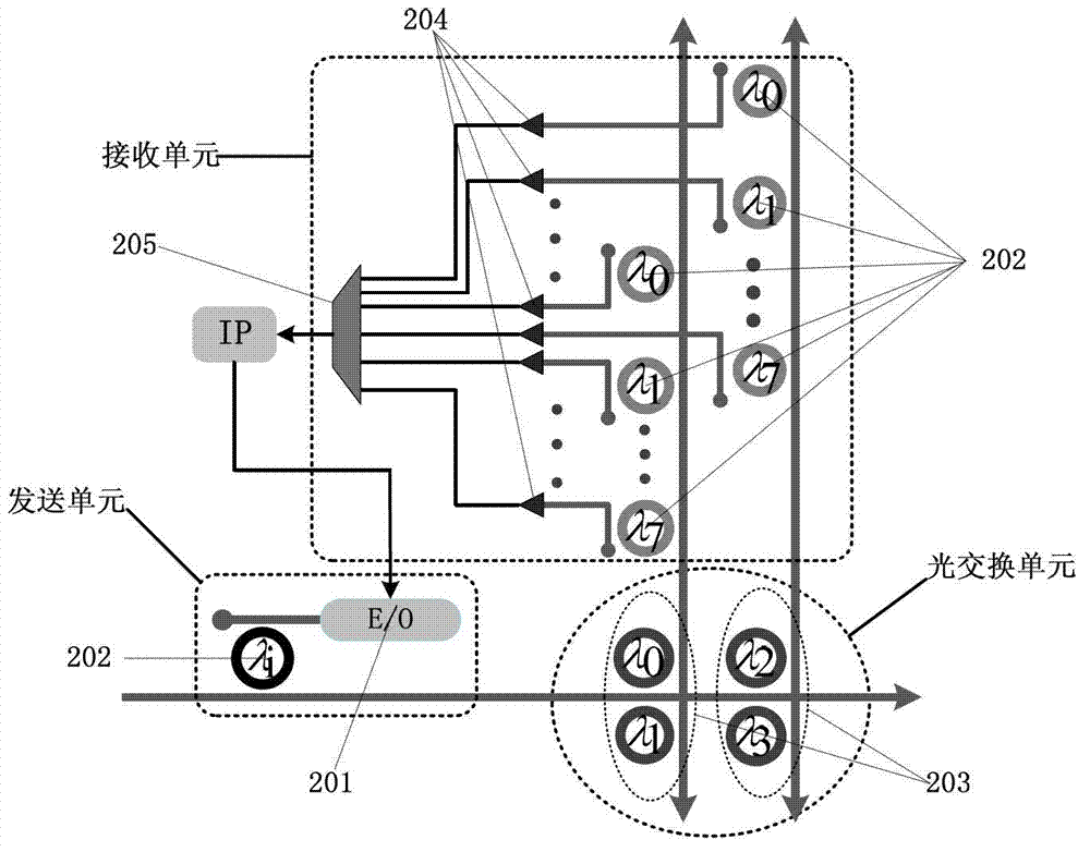
[0033] refer to figure 1 , the optical network-on-chip system for non-blocking communication proposed by the present invention includes two parts: an optical transmission network and an electrical control network, and the scale of the optical network-on-chip system is 4×4. Among them, the optical transmission network is used to transmit the wavelength λ 0 ,λ 1 ,λ 2 ,λ 3 ,λ 4 ,λ 5 ,λ 6 ,λ 7 optical information, it includes 16 nodes 101, the 16 nodes are evenly and regularly arranged from left to right and from bottom to top, the nodes are connected by waveguides and form a Torus topology, and each node includes a An IP core 102 that also processes electrical information and electrical control information, a sending unit 103,...


PUM


Abstract

The invention discloses an optical on-chip network system of non-blocking communication and a communication method thereof and mainly solves the blocking problem of the existing optical on-chip network system. The optical on-chip network system comprises a light transmission network and an electric control network; each node in the light transmission network comprises an IP (Internet Protocol) core, a sending unit, a receiving unit and a light exchanging device, wherein the sending length of each sending unit is fixed and the light exchanging device is formed by light vertical switches; and the inner structures of all the receiving units are the same. The communication method comprises the following steps of: firstly, establishing a two-dimensional coordinate system for the light transmission network and reading coordinates of a source node and a target node; secondly, opening a needed micro-ring resonator by the electric control network according to the source node and the target node; and finally, transmitting the light information to the target node by the light transmission network to be processed, and closing the opened micro-ring resonator. The optical on-chip network system disclosed by the invention combines a wavelength division multiplexing technology, a space division multiplexing technology and a light circuit exchanging technology to realize the non-blocking communication of the IP cores and improve the resource utilization rate and the throughput performance of the network.

Description

technical field [0001] The invention belongs to the technical field of communication, in particular to an optical on-chip network system for non-blocking communication, which supports non-blocking communication between on-chip processors, improves network resource utilization and delay throughput performance, and supports many-to-one non-blocking communication . Background technique [0002] The system-on-chip based on the bus structure is to integrate multiple IP cores on the chip through the bus interconnection. In the process of developing towards multi-core and heterogeneity, the system-on-chip has low communication efficiency due to the bus structure. Problems such as poor scalability have gradually become the bottleneck limiting the performance of on-chip communication. Therefore, the network on a chip came into being. The core idea of ​​the network on chip is to transplant the computer network technology into the chip design, so as to completely solve the problems c...

Claims


Application Information

Patent Timeline
Patent Type & Authority Applications(China)
IPC IPC(8): H04Q11/00H04B10/00
Inventor 陈可顾华玺杨银堂王琨陈峥李慧
Owner XIDIAN UNIV
Why Eureka
Try Eureka