Column address distributor circuit suitable for different types of FPGA (field programmable gate array) circuit programming

A column address and distributor technology, applied in electrical program control, program control in sequence/logic controllers, etc., can solve the problems of large delay and long circuit layout, save area, save layout area, and reduce delay time Effect

Active Publication Date: 2015-03-25
SOI MICRO CO LTD
View PDF8 Cites 0 Cited by
  • Summary
  • Abstract
  • Description
  • Claims
  • Application Information

AI Technical Summary

Problems solved by technology

[0010] In view of this, the main purpose of the present invention is to provide a kind of column address allocator circuit applicable to different types of FPGA circuit programming, to solve the large-scale multi-module FPGA configuration circuit in the column address allocator circuit layout large delay long problem, To achieve the purpose of saving area and increasing working frequency

Method used


Image

  • Column address distributor circuit suitable for different types of FPGA (field programmable gate array) circuit programming
  • Column address distributor circuit suitable for different types of FPGA (field programmable gate array) circuit programming
  • Column address distributor circuit suitable for different types of FPGA (field programmable gate array) circuit programming

Examples


Embodiment 1

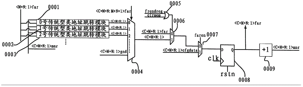
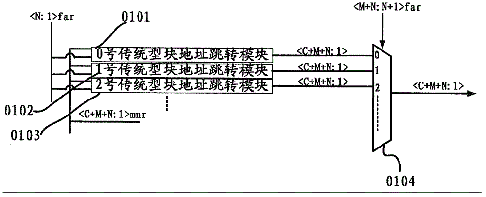
[0059] Figure 6 , Figure 7 , Figure 8 is a schematic structural diagram of the column address allocator circuit according to the first embodiment of the present invention. Figure 7 yes Figure 6 subgraph of Figure 8 yes Figure 7 subgraph of .

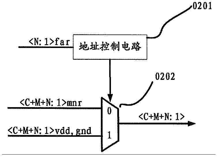
[0060] Figure 6 Among them, 1001, 1002, and 1003 represent the new class address jump modules, 1001 is the module for programming the first class in FPGA, 1002 is the module for programming the second class, and 1003 is the module for programming the third class Module, according to the actual FPGA, the number of classes that need to be programmed is also different, but the structure of each class address jump module is similar and different; 1004 is a group of parallel multiple The channel selector circuit, their input is the output of each class address jump module, according to the control signal of the multiplexer, that is, the bit of the address to judge the current multiplexer Which input of the select...

Embodiment 2

[0064] In the second embodiment, the FPGA for which the column address allocator circuit will be used has three types of circuits: an input-output block (IOB), a logic block (LB) and a global clock block (GB). The input-output block (IOB) has two circuit blocks, each with 19 programming bit lines; the logic block (LB) has 14 circuit blocks, and each circuit block has 26 programming bit lines; the global clock module ( GB) has 3 circuit blocks, and each circuit block has 8 programming bit lines.

[0065] In this embodiment, the FPGA has 3 class circuits, which are 2 after subtracting 1, and the binary expression is 'b10, which is at least 2-bit binary expression, that is, C=2; the number of block circuits contained in each class circuit is different, up to 14 , after subtracting 1, it is 13, that is, 'b1101, at least 4-bit binary expression, that is, M=4; the number of bit lines of each block of a class circuit is different, the maximum value is 26, and subtracting 1 is 25,...


PUM


Abstract

The invention discloses a column address distributor circuit suitable for different types of FPGA (field programmable gate array) circuit programming, comprising a column last signal and zero clearing signal control circuit, a far signal and address skip signal selecting circuit, a classful address skip signal selecting circuit, a cfgdata signal and address skip signal selecting circuit, a far signal output retaining circuit, a mnr signal generating circuit, a first classful address skip module and a second classful address skip module. By utilizing the column address distributor circuit, the problem that the column address distributor in a large-scale multiple-module FPGA configuration circuit has large circuit layout and long time delay is solved, and the purposes of saving area and improving the working frequency are achieved.

Description

technical field [0001] The invention relates to the field programmable gate array (FPGA) technical field, more specifically to a column address allocator circuit suitable for programming of different types of FPGA circuits. Background technique [0002] Field Programmable Gate Array (FPGA) has become an important technology for realizing modern circuits and systems due to its user programmability and low development cost. Compared with Application Specific Integrated Circuits (ASIC for short), FPGA's low R&D cost and short development cycle make it an important core technology for realizing modern digital circuits and systems, and its market share is also in the increase yearly. As the column address allocator circuit used for programming in FPGA, its design directly affects the programming speed and efficiency of FPGA to a large extent. [0003] Generally speaking, the programming address of FPGA is divided into three parts: class address, block address and bit line addre...

Claims


Application Information

Patent Timeline
Patent Type & Authority Patents(China)
IPC IPC(8): G05B19/05
Inventor 赵岩于芳韩小炜吴利华
Owner SOI MICRO CO LTD
Why Eureka
Try Eureka