LDMOS device with stepped multiple discontinuous filed plate and manufacturing method for LDMOS device

A stepped, field plate technology, used in semiconductor/solid-state device manufacturing, semiconductor devices, electrical components, etc., can solve the problem of single distance between the field plate and the device surface.

Active Publication Date: 2012-11-21
INNOGRATION SUZHOU
View PDF4 Cites 21 Cited by
  • Summary
  • Abstract
  • Description
  • Claims
  • Application Information

AI Technical Summary

Problems solved by technology

However, the commonly used single field plate technology has great limitations, because the distance between the horizontal part of the field plate and the semiconduc...

Method used


Image

  • LDMOS device with stepped multiple discontinuous filed plate and manufacturing method for LDMOS device
  • LDMOS device with stepped multiple discontinuous filed plate and manufacturing method for LDMOS device
  • LDMOS device with stepped multiple discontinuous filed plate and manufacturing method for LDMOS device

Examples


Embodiment

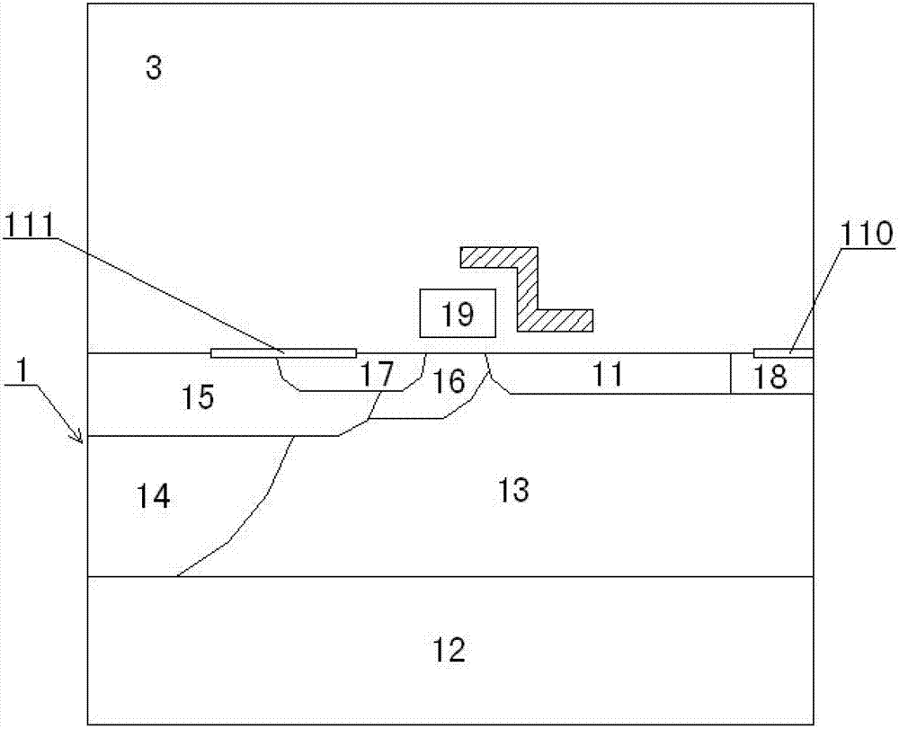
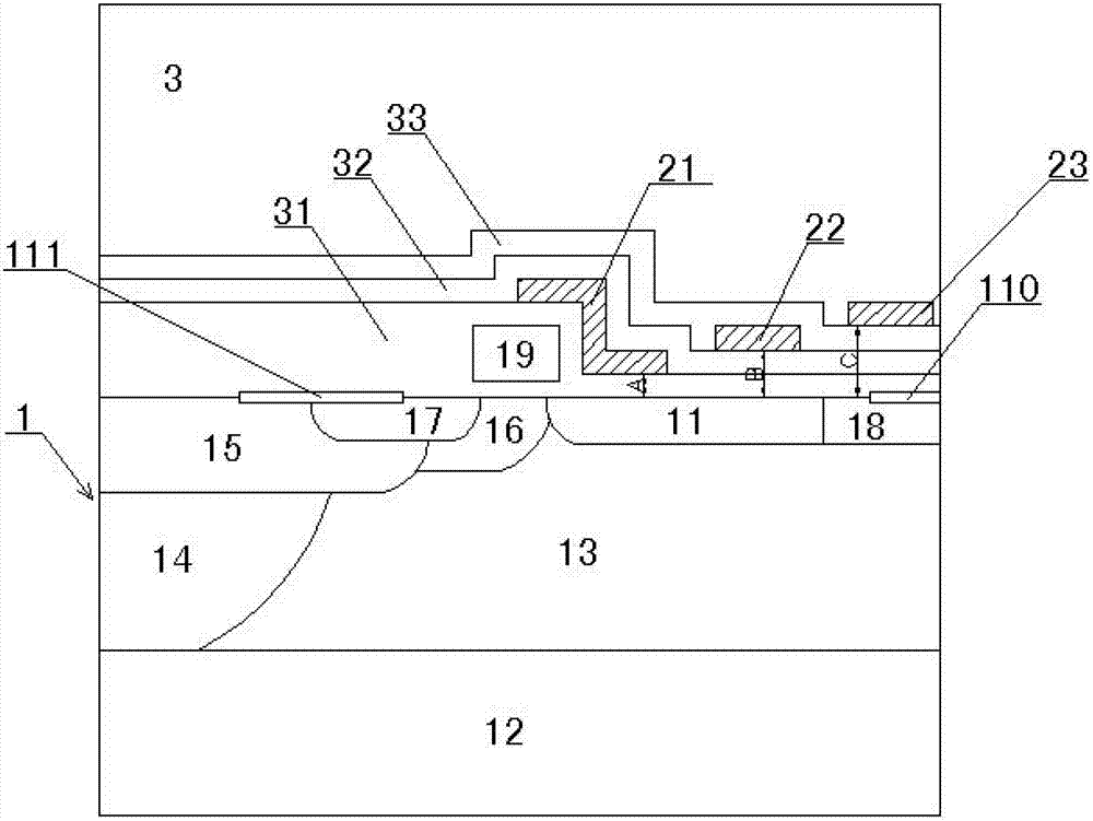
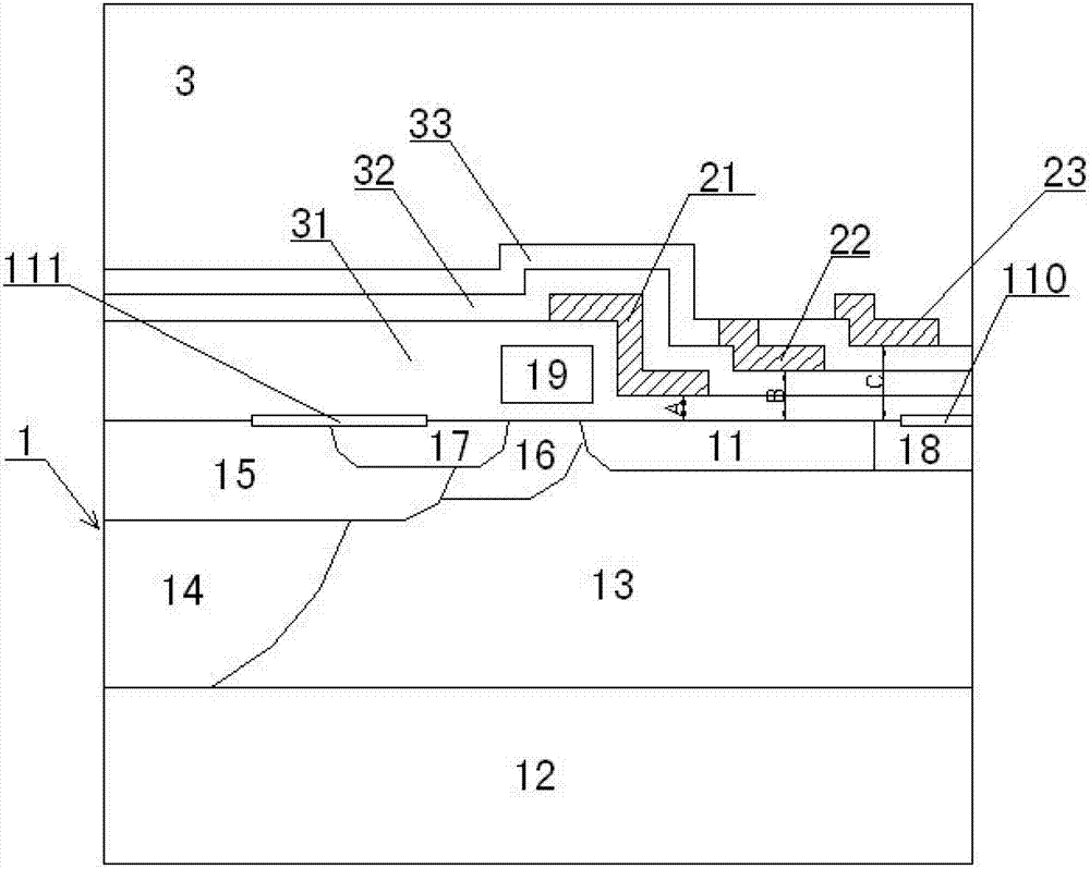
[0032] The structure of the LDMOS device with stepped multiple discontinuous field plates described in this embodiment is as follows figure 2 As shown, it includes a semiconductor body 1, the semiconductor body 1 includes a lowermost P-type heavily doped substrate 12, a P-type epitaxial layer 13 on the P-type heavily doped substrate 12, and an uppermost semiconductor dielectric layer 3 A P-type heavily doped source region 15, a P-type doped channel region 16, an N-type doped drain drift region 11 and an N-type heavily doped drain region 18 are formed between the P-type epitaxial layer 13 and the semiconductor dielectric layer 3 , where the P-type heavily doped source region 15 and the P-type doped channel region 16 are connected to form an N-type heavily doped source region 17 . Between the P-type heavily doped source region 15 and the P-type heavily doped substrate, a P-type doped connection or a trench 14 filled with a conductor is arranged, and the P-type doping in the tre...


PUM


Abstract

The invention discloses an LDMS (Laterally Diffused Metal Oxide Semiconductor) device with a stepped multiple discontinuous filed plate and a manufacturing method for the LDMS device. The LDMS device comprises a semiconductor body, wherein the semiconductor body comprises a semiconductor substrate region, a semiconductor epitaxial layer and a semiconductor medium layer which are sequentially arranged from bottom to top; a grid extending along a channel and at least two field plates are arranged in the semiconductor medium layer; at least two field plates are sequentially arranged in a horizontal direction from the grid to a leakage-drift region; a first field plate adjacent to the grid horizontally extends in the leakage-drift region; field plates which are not adjacent to the grid are respectively in a horizontal strip shape; the distance between every two field plates is greater than zero; the distance between a second field plate adjacent to the first field plate and the leakage-drift region is greater than the distance between a horizontally-extending part of the first field plate and the leakage-drift region; and the distance between other horizontal strip field plates and the leakage-drift region is gradually increased. According to the LDMS device disclosed by the invention, the contradiction between source and drain breakdown voltage and the optimal requirement of a conducting resistor is relieved and the performance of the LDMS device is improved.

Description

technical field [0001] The invention relates to an LDMOS device with stepped multiple discontinuous field plates and a corresponding processing method thereof. Background technique [0002] In power LDMOS devices, it is required to reduce the source-drain on-resistance Rds of the device as low as possible on the premise of satisfying the source-drain breakdown voltage BVdss. The existing technology improves the working efficiency of the device by reducing the power consumption of the device. However, the optimization requirements of source-drain breakdown voltage and on-resistance are contradictory. In radio frequency LDMOS power devices, field plate technology is often used to alleviate this contradiction. However, the commonly used single field plate technology has great limitations, because the distance between the horizontal part of the field plate and the semiconductor surface is constant, such as figure 1 As shown, but the ideal field plate requires that the distance ...

Claims


Application Information

Patent Timeline
IPC IPC(8): H01L29/78H01L29/40H01L21/336
CPCH01L29/66659H01L29/78H01L29/4175H01L29/7835H01L29/404H01L29/40
Inventor 马强
Owner INNOGRATION SUZHOU
Why Eureka
Try Eureka