Low-temperature CMOS (Complementary Metal-Oxide-Semiconductor Transistor) modeling method

A modeling method, low temperature technology, applied in the field of CMOS modeling

Inactive Publication Date: 2012-11-28
SHANGHAI INST OF TECHNICAL PHYSICS - CHINESE ACAD OF SCI
View PDF0 Cites 8 Cited by
  • Summary
  • Abstract
  • Description
  • Claims
  • Application Information

AI Technical Summary

Problems solved by technology

This modeling does not address low temperature applications and requirements, but is based on a simple analytical model to evaluate the single event transient susceptibility of each gate in the complex circuit

Method used


Image

  • Low-temperature CMOS (Complementary Metal-Oxide-Semiconductor Transistor) modeling method
  • Low-temperature CMOS (Complementary Metal-Oxide-Semiconductor Transistor) modeling method
  • Low-temperature CMOS (Complementary Metal-Oxide-Semiconductor Transistor) modeling method

Examples


Embodiment 1

[0038] The measurement methods of various parameters of the low temperature model are as follows:

[0039] In order to extract the model, the NMOS tube needs to be connected into a four-terminal device, SOURCE, DRAIN, GATE, SUBSTRATE, the substrate is grounded, the initial voltage of Vgs is 0.7 volts, the change step is 0.86 volts, and the initial voltage of Vds is 0 volts. The change step size is 0.05 volts, and the characteristic curve of Vds-Id can be drawn after the scanning is completed (the abscissa is Vds, the unit is volts; the ordinate is Id, the unit is Ampere).

[0040] When performing Vgs-Id scanning, the initial voltage of Vgs is 0 volts, the change step is 0.05 volts, and Vds is 0.1 volts and 5 volts.

[0041] Test of junction capacitance Cgg: For NMOS four-terminal devices, connect SOURCE, DRAIN, and SUBSTRATE to the High end of CV590meter, and connect GATE to the Low end of CV590meter. The Vgs scanning range is -5 volts - 5 volts, the initial voltage is 5 volt...

Embodiment 2

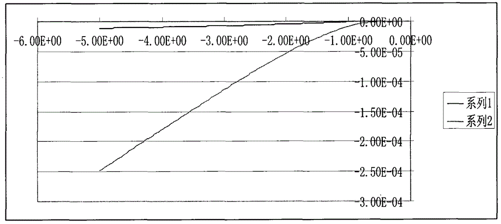
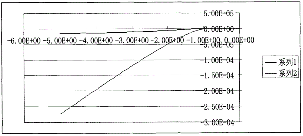
[0043] For threshold voltage changes, figure 1 and figure 2 It is the Vgs-Id characteristic curve of PMOS tube 0.6 / 0.55 at room temperature and low temperature 77K. Using the Vgs-Id characteristic curve, it can be concluded from the test results that as the temperature decreases, the threshold voltage V T Increase. The specific increase range is 1mV / 1°C.

Embodiment 3

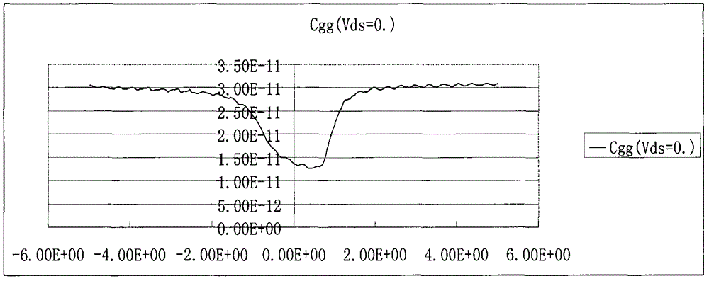
[0045] For capacitance modification, image 3 and Figure 4 It is the Cgg-Vgs curve of NMOS tube 100 / 100 Dewar normal temperature 300K and Dewar low temperature 77K. It can be seen from the above two figures that the Cgg-Vgs curve has a small drop as the temperature decreases, but the change is not obvious. Its specific capacitance value variation is 5% smaller.


PUM


Abstract

The invention discloses a CMOS (Complementary Metal-Oxide-Semiconductor Transistor) modeling method at a low temperature of being lower than 77 K. The method takes a BSIM3 (Berkeley Short-channel isolated gate field effect transistor Model 3) as a base; a model parameter with the pertinence is respectively selected from a BSIM3 model according to a physical definition that the model parameter is changed along the temperature and a counting expression correction term is added; an initial value of a correction coefficient is determined according to a test result; the initial value of the correction coefficient is substituted into the BSIM3 model; and the model parameter is debugged and simulated. The model parameter needing to be tested comprises Vgs-Id, Cgg-Vgs, Vds-Id, Cgc-Vgs, a high resistance HR and a low-temperature 77-K property of a poly1 resistor. BsimPro software is used for substituting a low-temperature test parameter result to enable a simulation curve to be accurately close to an actual low-temperature test property curve, more simply and rapidly finish the modeling of an MOS (Metal-Oxide-Semiconductor Transistor) transistor at the low temperature of 77 K and improve the low-temperature design capability of a special integrated circuit.

Description

technical field [0001] The invention relates to a CMOS modeling method, in particular to a method for establishing a 0.5 micron process CMOS model at a low temperature of 77K. Background technique [0002] For infrared detectors, especially photoconductive infrared detectors, in order to reduce the overall noise of the system, it is necessary to connect the readout circuit to the infrared detector at close range, which requires the circuit to work normally at low temperature. The models are all for normal temperature, and there is no low temperature model of about 77K, which leads to inaccurate low temperature circuit design. In order to solve this problem, it is necessary to establish a practical low temperature model. At present, the methods for establishing the MOS tube model are generally divided into two types: forward propagation (forward propagation) and backward propagation (backward propagation). The main advantage of the forward propagation method is that the pro...

Claims


Application Information

Patent Timeline
Patent Type & Authority Applications(China)
IPC IPC(8): G06F17/50
Inventor 袁红辉陈永平陈世军刘强徐星丁毅王欣
Owner SHANGHAI INST OF TECHNICAL PHYSICS - CHINESE ACAD OF SCI
Why Eureka
Try Eureka