Stress sensor transfer method used for measuring wafer level packaging stress

A stress sensor, wafer-level packaging technology, applied in the fields of packaging and measurement, and integrated circuit manufacturing, can solve the problems of high processing cost, high development cost, and high development cost of integrated circuit process lines

Inactive Publication Date: 2012-11-28
SHANGHAI INST OF MICROSYSTEM & INFORMATION TECH CHINESE ACAD OF SCI
View PDF1 Cites 0 Cited by
  • Summary
  • Abstract
  • Description
  • Claims
  • Application Information

AI Technical Summary

Problems solved by technology

The processing cost of 8-inch or 12-inch integrated circuit process line is high, and the development cost is high due to the small amount of test wafers
High development costs limit the application of stress sensors in wafer-level packaging

Method used


Image

  • Stress sensor transfer method used for measuring wafer level packaging stress
  • Stress sensor transfer method used for measuring wafer level packaging stress
  • Stress sensor transfer method used for measuring wafer level packaging stress

Examples


Embodiment Construction

[0036] Below in conjunction with specific embodiment, further illustrate the present invention. It should be understood that these examples are only used to illustrate the present invention and are not intended to limit the scope of the present invention. In addition, it should be understood that after reading the teachings of the present invention, those skilled in the art can make various changes or modifications to the present invention, and these equivalent forms also fall within the scope defined by the appended claims of the present application.

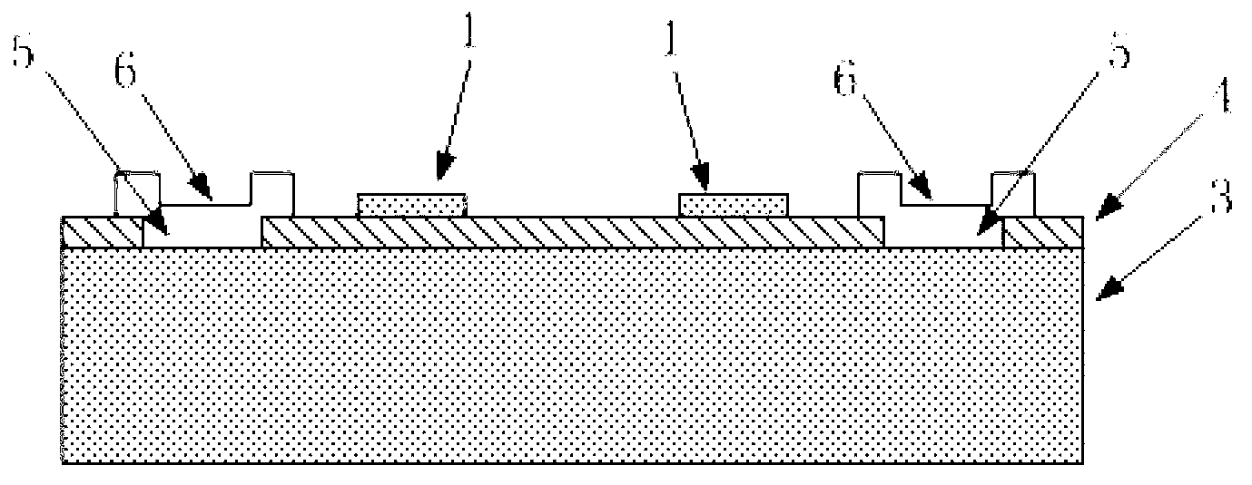
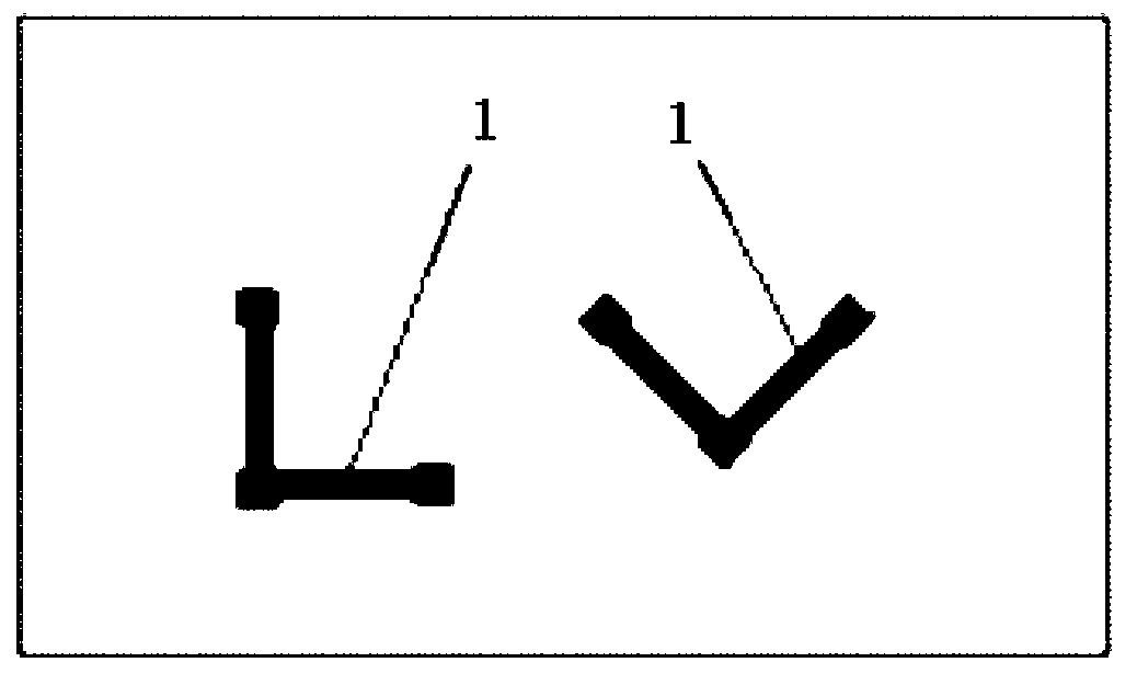
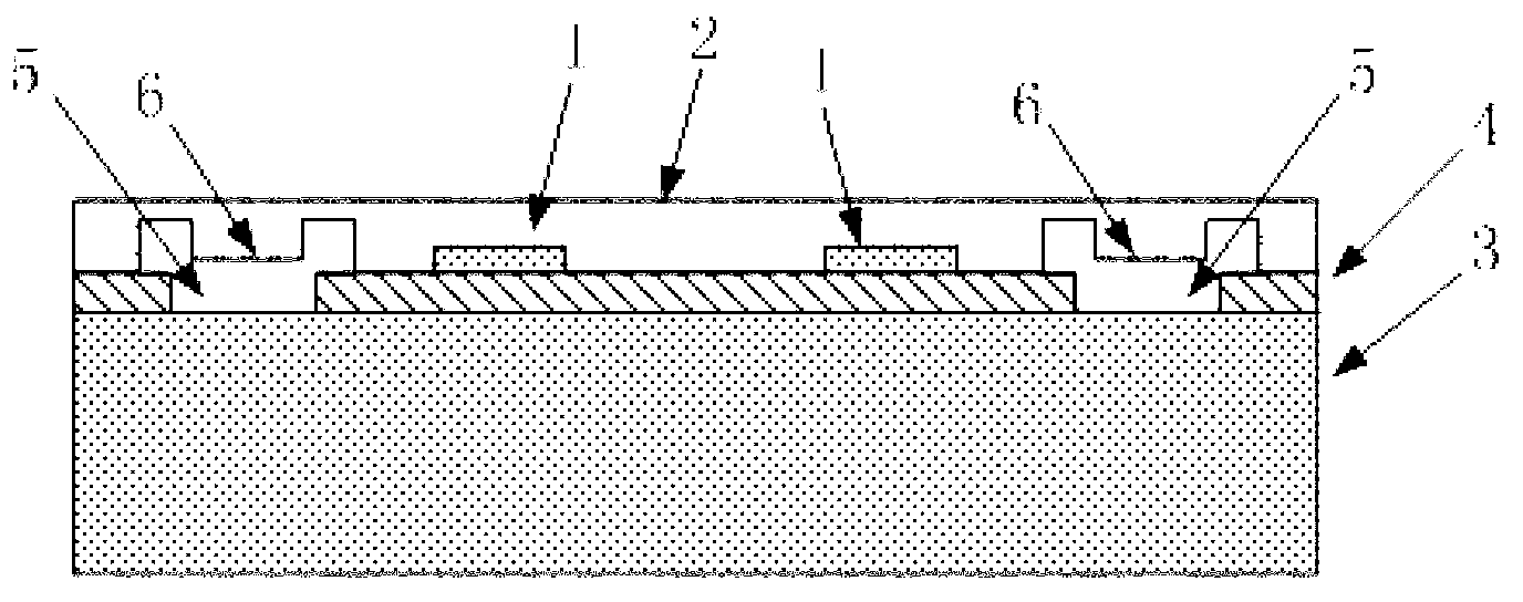
[0037] Embodiments of the present invention relate to a stress sensor transfer method for wafer-level packaging stress measurement, including the following steps: first, a dedicated test chip is fabricated, a stress sensor is fabricated on the test chip, and the size of the test chip and the arrangement of the pads are consistent with The chip to be packaged is the same; the test chip is packaged with the package process to be ...


PUM

PropertyMeasurementUnit
Thicknessaaaaaaaaaa

Abstract

The invention relates to a stress sensor transfer method used for measuring the wafer level packaging stress, which comprises the following steps of: manufacturing a stress sensor on top layer silicon of an SOI (Silicon-On-Insulator) silicon wafer; attaching the stress sensor to a test wafer with the same size to a wafer to be packaged to the stress sensor in a face-to-face way by using an organic glue film; and removing substrate silicon of the stress sensor through etching, and transferring a chip unit of the stress sensor to the test wafer. In the invention, the stress sensor is manufactured on a small-size silicon wafer, the processing cost of the small-size silicon wafer is obviously lower than that of a large-size silicon wafer, a chip cut from one sensor wafer can meet the use level of a plurality of test wafers, and the use cost is far lower than that of directly manufactured large-size test wafers.

Description

technical field [0001] The invention relates to the technical fields of integrated circuit manufacturing, packaging and measurement, in particular to a stress sensor transfer method for wafer-level packaging stress measurement. Background technique [0002] The packaging process of the integrated circuit introduces stress in the integrated circuit chip. Since the carrier mobility of semiconductor materials such as silicon will change with stress, packaging stress will have a significant impact on the performance of integrated circuits. In addition, material fatigue caused by package stress changing with temperature is an important cause of integrated circuit failure. It is generally necessary to reduce packaging stress through optimization of materials, packaging structures, and processes. [0003] The stress sensor fabricated by utilizing the piezoresistive effect of silicon is a powerful tool for package stress measurement. The piezoresistive stress sensor uses the piez...

Claims


Application Information

Patent Timeline
IPC IPC(8): H01L21/66
Inventor 杨恒豆传国吴燕红李昕欣王跃林
Owner SHANGHAI INST OF MICROSYSTEM & INFORMATION TECH CHINESE ACAD OF SCI
Why Eureka
Try Eureka