Back-illuminated CMOS (complementary metal oxide semiconductor) image sensor

An image sensor, back-illuminated technology, applied in the field of back-illuminated CMOS image sensors, can solve the problems of low photon conversion efficiency, pixel cross-interference, etc., to achieve the effect of improving imaging quality, reducing the probability of escape, and improving photon conversion efficiency

Active Publication Date: 2012-11-28
OMNIVISION TECH (SHANGHAI) CO LTD
View PDF6 Cites 3 Cited by
  • Summary
  • Abstract
  • Description
  • Claims
  • Application Information

AI Technical Summary

Problems solved by technology

That is to say, the structure of the traditional front-illuminated CMOS image sensor makes the incident light need to pass through the dielectric layer (dielectric layer) and the metal layer (metal layer) before reaching the photo-sensing area, which leads to the traditional CMOS image sensor Need to face low photon conversion efficiency (quantum efficiency), serious cross talk between pixels (cross talk) and dark current (dark current), etc.

Method used


Image

  • Back-illuminated CMOS (complementary metal oxide semiconductor) image sensor
  • Back-illuminated CMOS (complementary metal oxide semiconductor) image sensor
  • Back-illuminated CMOS (complementary metal oxide semiconductor) image sensor

Examples


Embodiment Construction

[0020] The back-illuminated CMOS image sensor provided by the present invention will be further described in detail below with reference to the drawings and specific embodiments. Advantages and features of the present invention will be apparent from the following description and claims. It should be noted that all the drawings are in a very simplified form, and are only used for the purpose of conveniently and clearly assisting in describing the embodiments of the present invention.

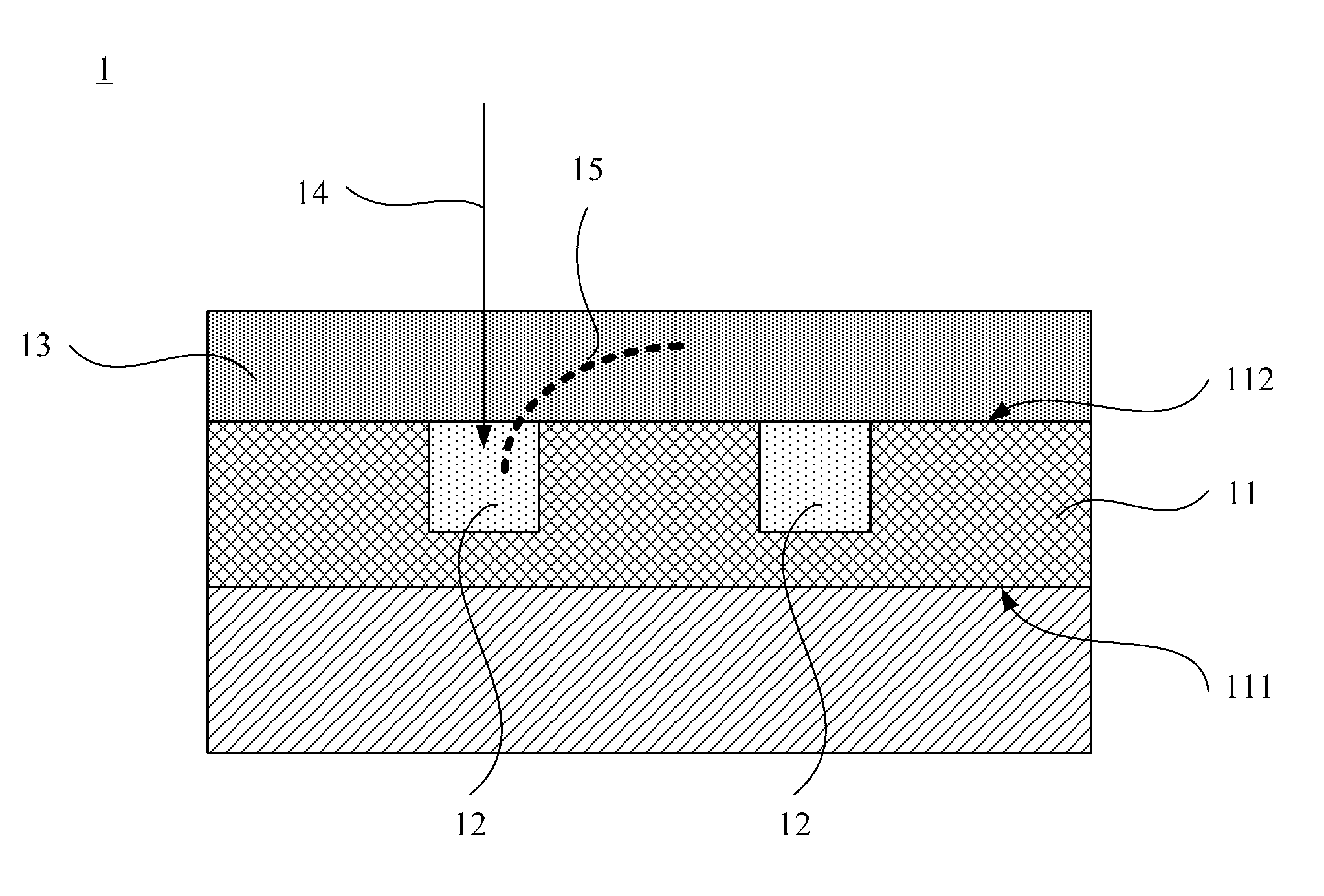
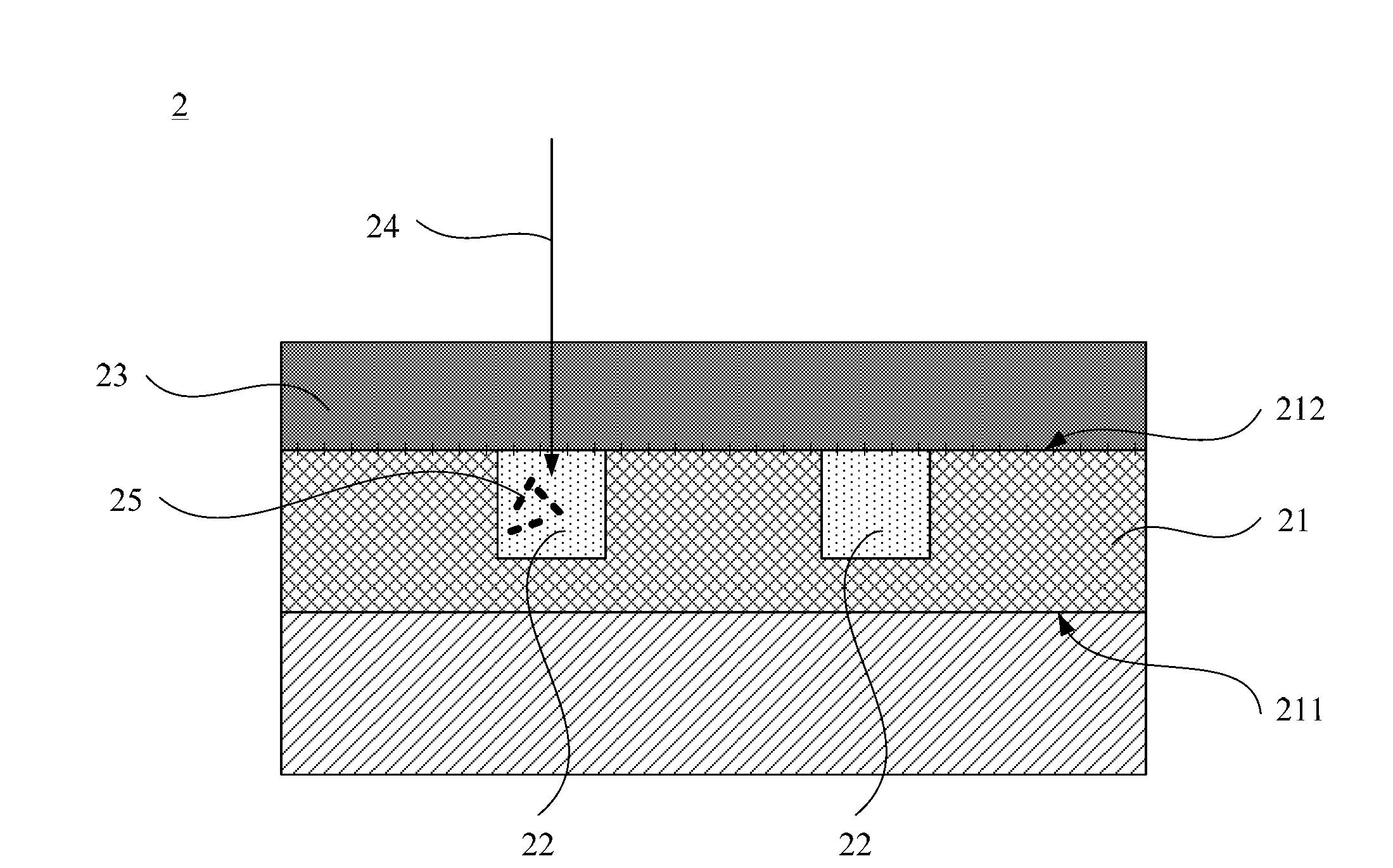
[0021] As mentioned in the background technology, the technology of back-illuminated CMOS image sensor is developed on the technology of front-illuminated CMOS image sensor. Some improvements have been made to low problems. like figure 1 As shown in , it is a schematic cross-sectional view of a conventional back-illuminated CMOS image sensor. The existing back-illuminated CMOS image sensor 1 includes:

[0022] A device wafer 11, the device wafer 11 has a front side 111 and a back side 112, a ...


PUM

PropertyMeasurementUnit
Thicknessaaaaaaaaaa

Abstract

The invention provides a back-illuminated CMOS (complementary metal oxide semiconductor) image sensor, comprising a device wafer and a positively-charged film layer, wherein the device wafer is provided with a front surface and a back surface, a photodiode is formed in the device wafer, and the photodiode is close to the back surface of the device wafer; and the positively-charged film layer covers the back surface of the device wafer. Via the positively-charged film layer, the potential barrier of an energy band close to the back surface of the device wafer is increased, and the difficulty in escaping from the photodiode of the electrons is increased, thus decreasing the probability that the electrons escape from the photodiode, and then increasing photon conversion efficiency and improving the imaging quality of the back-illuminated CMOS image sensor.

Description

technical field [0001] The invention relates to the technical field of image sensors, in particular to a back-illuminated CMOS image sensor. Background technique [0002] A digital camera is an electronic product widely used today, and an image sensor is included in the digital camera, which is used to convert light into electric charge. Image sensors can be divided into charge-coupled device (Charge-Coupled Device) image sensors (commonly known as CCD image sensors) and CMOS (Complementary Metal Oxide Semiconductor) image sensors according to the principle they use. CMOS image sensors are based on complementary metal Manufactured using oxide semiconductor (CMOS) technology. Since the CMOS image sensor is manufactured using a traditional CMOS circuit process, the image sensor and its required peripheral circuits can be integrated. [0003] Traditional CMOS image sensors use Front Side Illumination (FSI) technology to manufacture pixels on the pixel array, and the incident ...

Claims


Application Information

Patent Timeline
IPC IPC(8): H01L27/146
Inventor 余兴肖海波费孝爱
Owner OMNIVISION TECH (SHANGHAI) CO LTD
Why Eureka
Try Eureka