Secondary pre-alignment device and pre-alignment method
What is AI technical title?
AI technical title is built by Patsnap AI team. It summarizes the technical point description of the patent document.
A technology for pre-aligning and mounting plates, which is applied in the direction of exposure devices, optics, instruments, etc.
Active Publication Date: 2014-12-17
SHANGHAI MICRO ELECTRONICS EQUIP (GRP) CO LTD
View PDF4 Cites 0 Cited by
Summary
Abstract
Description
Claims
Application Information
AI Technical Summary
This helps you quickly interpret patents by identifying the three key elements:
Problems solved by technology
Method used
Benefits of technology
Problems solved by technology
Therefore, if the heat source is arranged on the main substrate, close to the projection objective lens and sensors of other subsystems, it will have a great impact on the surrounding temperature field
Similarly, if the heat source is arranged on the exercise platform, it will have a great impact on the temperature field of the exercise platform
Method used
Image
Click on the blue label to locate the original text in one second.
Reading with bidirectional positioning of images and text.
Examples
Embodiment 1
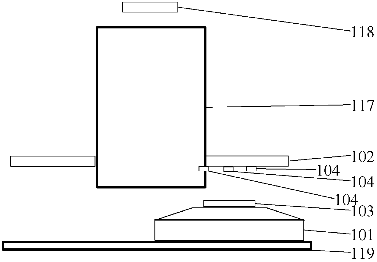
[0046] see Figure 1-Figure 7 , this secondary pre-alignment device is set between the moving table 101 and the main substrate 102, and is used to perform secondary pre-alignment on the wafer 103 placed on the moving table 101, and the wafer 103 is placed on the moving On stage 101. A projection objective lens 117 is disposed on the main substrate 102 , and a mask table 118 is disposed above the projection objective lens 117 . The exercise table 101 is arranged on a marble slab 119 .
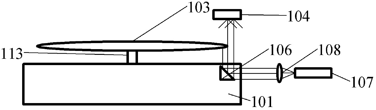
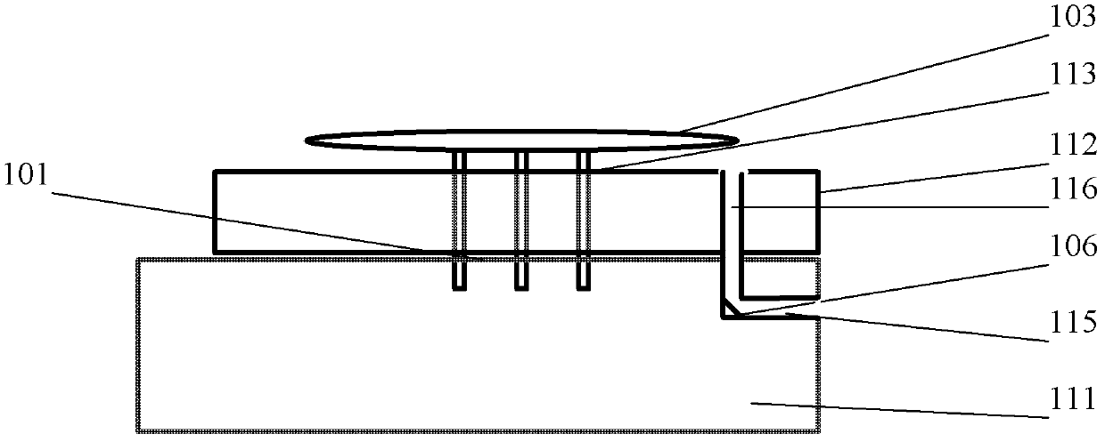
[0047] The secondary pre-alignment device includes three area array CCD104 (including CCD1, CCD2 and CCD3), three groups of optical path systems (including the first group of optical path systems, the second group of optical path systems and the third group of optical path systems) and an image processing device 105. The full name of the area array CCD104 refers to Charge-coupled device, which refers to a charge-coupled device. The three sets of optical path systems respectively project thre...
Embodiment 2
[0077] The difference between this embodiment and embodiment 1 is:
[0078] see Figure 8-Figure 9 , Figure 8 and Figure 9 Among them, 218-mask stage, 217-projection objective lens, 220-second 45-degree triangular mirror, 202-main substrate, 204-array CCD, 203-wafer, 201-moving stage, 219-marble plate, 224 -Area array mounting plate. The difference between this embodiment and Embodiment 1 is that each group of optical path systems includes a first 45-degree triangular reflector 206 and a second 45-degree triangular reflector 220 that receive light beams from the light source, and the first 45-degree triangular reflector 206 Corresponding to the second 45-degree triangular mirror 220, it is arranged on the upper and lower sides of an edge of the wafer 203. The edge image of circle 3 is projected to the corresponding area array CCD204. The first 45-degree triangular reflector 206 is distributed in the interior of the moving table 201 in a triangular shape, and the second ...
Embodiment 3
[0080] see Figure 10 , Figure 10 Among them, 301-motion table, 306-first 45-degree triangular mirror, 307-light source, 308-light path collimation mechanism, 309-light source installation bracket, 314-mechanical transmission hand, 317-projection objective lens, 319-marble plate. The difference between this embodiment and Embodiment 1 is that the three groups of optical path systems are the first group of optical path systems, the second group of optical path systems and the third group of optical path systems, and the three groups of optical path systems share a light source 307 and an optical path collimation mechanism 308, and the first group of optical path systems also includes a triangular reflector 321 of 2 / 3 light transmittance, the second group of optical path systems also includes a triangular reflector 322 of 1 / 2 light transmittance, and the third group of optical path systems also includes a third 45 degree triangular reflector 323. The light source 307 is insta...
PUM
Abstract
The invention relates to a secondary pre-alignment device. The secondary pre-alignment device is arranged between a movement station and a main substrate, is used for carrying out secondary pre-alignment on a wafer placed on the movement station and comprises three area array CCDs (Charge Coupled Device), three groups of optical path systems and an image processor. The three groups of optical path systems are used for respectively projecting three edge images of the wafer to the corresponding area array CCDs; a light source required by the three groups of optical path systems is arranged outside the movement station; the three area array CCDs are connected with the image processor; and the image processor is used for processing wafer edge image information from the three area array CCDs and then calculating the residual eccentric deviation of the wafer. A direct irradiation principle is adopted and the light source and the area array CCDs are respectively arranged at both sides of the wafer, so that not only is the accuracy higher, but also the secondary pre-alignment device is difficult to influence by the installing angle; and moreover, the design optical path is simple and the light energy dissipation is low. Moreover, the light source is arranged far away from key parts sensitive to a heat source, such as a projection objective, an objective, the main substrate, the movement station and the like, so that the performance stability of the secondary pre-alignment device is improved and the alignment accuracy is further improved.
Description
technical field [0001] The invention relates to the field of semiconductor photolithography, in particular to a wafer secondary alignment device and an alignment method thereof. Background technique [0002] At present, with the continuous shrinking of the critical size of the lithography machine, the requirements for the internal world of the lithography machine are also continuously increasing. The secondary pre-alignment measurement device measures the residual eccentricity of the wafer reaching the internal world, making the way of moving the stage to compensate becomes a development trend. During the transfer of the wafer from the cassette to the motion table, after pre-alignment, the eccentricity is about 10 μm and the deviation is about 150 μrad. The edge of the wafer is composed of most of the arc and the notch or flat edge that plays an orientation role. After centering and orientation, it is then transferred to the handover position above the motion table. The han...
Claims
Application Information
Patent Timeline
Application Date:The date an application was filed.
Publication Date:The date a patent or application was officially published.
First Publication Date:The earliest publication date of a patent with the same application number.
Issue Date:Publication date of the patent grant document.
PCT Entry Date:The Entry date of PCT National Phase.
Estimated Expiry Date:The statutory expiry date of a patent right according to the Patent Law, and it is the longest term of protection that the patent right can achieve without the termination of the patent right due to other reasons(Term extension factor has been taken into account ).
Invalid Date:Actual expiry date is based on effective date or publication date of legal transaction data of invalid patent.
Patent Type & AuthorityPatents(China)
IPC IPC(8): G03F9/00G03F7/20
Inventor郑教增宋平徐伟
OwnerSHANGHAI MICRO ELECTRONICS EQUIP (GRP) CO LTD

