Fin type field-effect transistor forming method

A fin-type field effect transistor and fin technology are applied in the directions of electrical components, semiconductor/solid-state device manufacturing, circuits, etc., which can solve the problem that the performance stability of the fin-type field effect transistor needs to be further improved, and achieve good penetration prevention effect. Guaranteed isolation effect and improved performance stability

Active Publication Date: 2015-07-01
SEMICON MFG INT (SHANGHAI) CORP
View PDF5 Cites 19 Cited by
  • Summary
  • Abstract
  • Description
  • Claims
  • Application Information

AI Technical Summary

Problems solved by technology

[0004] However, with the further shrinking of the process node, the performance stability of the fin field effect transistor formed by the existing technology needs to be further improved

Method used


Image

  • Fin type field-effect transistor forming method
  • Fin type field-effect transistor forming method
  • Fin type field-effect transistor forming method

Examples


Embodiment Construction

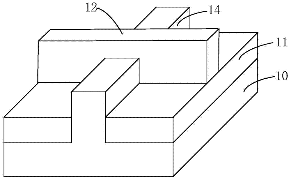
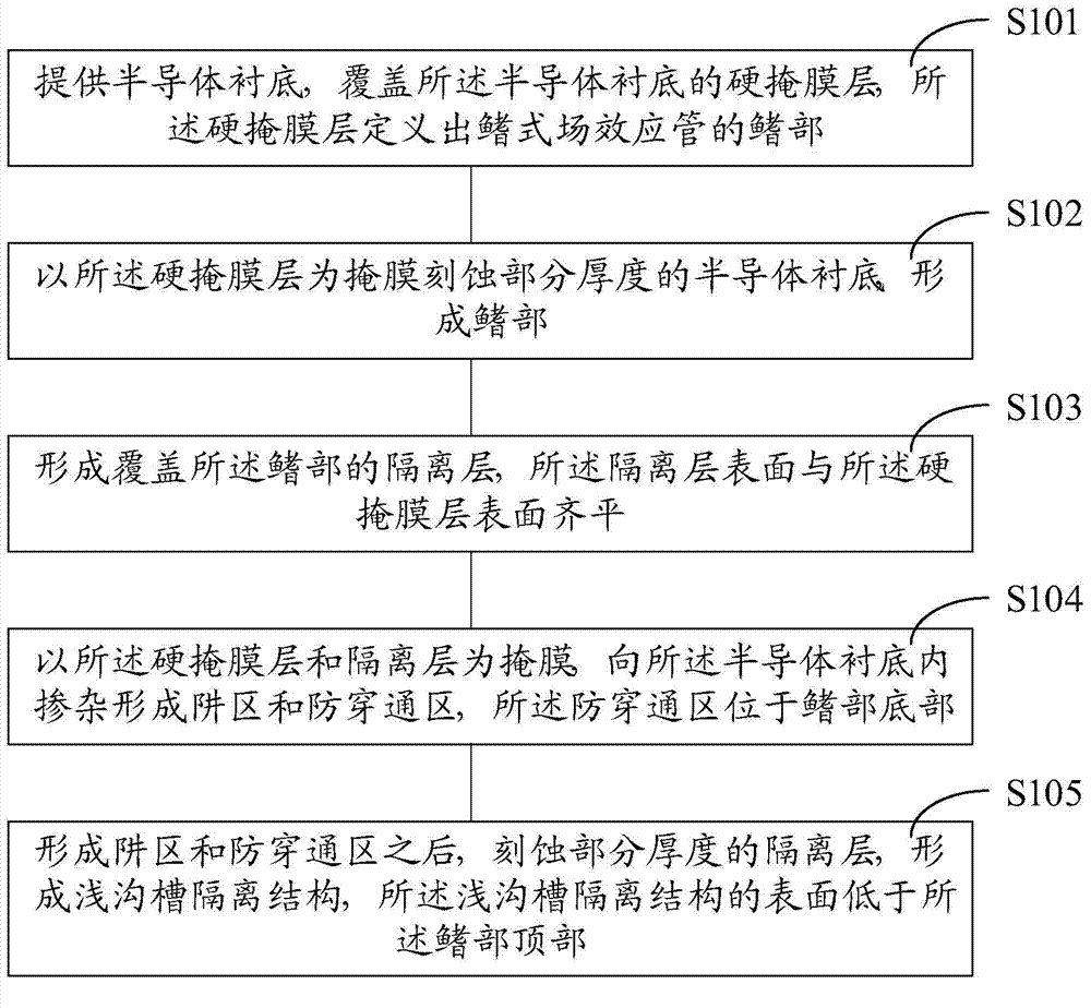
[0027] As described in the background art, the performance stability of the fin-type FET formed in the prior art needs to be further improved.

[0028] After research, it is found that the above phenomenon is caused by the following factors: one is the ion concentration of the punch-through region at the bottom of the fin; the second is the quality of the fin; and the third is the depth of the well region doping.

[0029] Through research, it is found that when forming fin-type FETs, if the semiconductor substrate is doped before the fins and shallow trench isolation structures are formed to form punch-through regions and well regions later, it can Avoid damage to the quality of the fins caused by ion doping, but the oxidation process and annealing process during the formation of the shallow trench structure are likely to cause ion diffusion (dose loss) in the anti-pierce area, resulting in low ion concentration in this area Is lower than the predetermined value, which makes the an...


PUM


Abstract

A fin type field-effect transistor forming method comprises the steps of providing a semiconductor substrate and a hard mask layer covering the semiconductor substrate, wherein the hard mask layer defines the fin portion of a fin type field-effect transistor; using the hard mask layer as a mask to etch a part of the semiconductor substrate to form the fin portion; forming an isolation layer covering the fin portion, wherein the surface of the isolation layer is flush with the surface of the hard mask layer; using the hard mask layer and the isolation layer as masks and forming a well region and a punchthrough-preventing region in the semiconductor substrate, wherein the punchthrough-preventing region is located at the bottom of the fin portion; etching a part of isolation layer after the well region and the punchthrough-preventing region are formed, forming a shallow-groove isolation structure, wherein the surface of the shallow-groove isolation structure is lower than the top of the fin portion. A formed fin type field-effect transistor is better in the punchthrough-preventing effect, the fin portion is better in quality, the isolation effect of the well region is better, and the performance stability of the fin type field-effect transistor is effectively improved.

Description

Technical field [0001] The invention relates to the technical field of semiconductor manufacturing, in particular to a method for forming a fin-type field effect transistor. Background technique [0002] With the continuous development of semiconductor process technology, process nodes are gradually reduced, high-K dielectric layers and metal gate electrodes have been widely used, and by forming metals with different work functions between the high-k dielectric layer and the metal gate electrode Obtain ideal threshold voltage and improve device performance. However, when the feature size (CD, Critical Dimension) of the device is further reduced, the structure of the conventional MOS field effect transistor can no longer meet the requirements for device performance, and the fin field effect transistor (Fin FET) has been replaced as a conventional device. Widespread concern. [0003] figure 1 The three-dimensional schematic diagram of a fin-type FET in the prior art is shown. Such...

Claims


Application Information

Patent Timeline
Patent Type & Authority Applications(China)
IPC IPC(8): H01L21/336H01L21/762
CPCH01L21/762H01L29/66795
Inventor 居建华施雪捷
Owner SEMICON MFG INT (SHANGHAI) CORP
Why Eureka
Try Eureka