Low voltage current mirror

A low-voltage current, input current technology, applied in the field of electronics, can solve the problems of waste of voltage margin, reduce output voltage swing, etc., to achieve the effect of increasing output voltage swing and high image accuracy

Inactive Publication Date: 2012-12-05
UNIV OF ELECTRONICS SCI & TECH OF CHINA
View PDF7 Cites 18 Cited by
  • Summary
  • Abstract
  • Description
  • Claims
  • Application Information

AI Technical Summary

Problems solved by technology

[0011] The purpose of the present invention is to solve the problem of reducing the output voltage swing due to the waste of a threshold voltage in the voltage margin of the existing cascode current mirror, and proposes a low-voltage current mirror

Method used


Image

  • Low voltage current mirror
  • Low voltage current mirror
  • Low voltage current mirror

Examples


Embodiment Construction

[0029] In the description of the following embodiments, all device parameters have been set, and the present invention is described and explained in more detail in combination with the simulation results of the embodiments. However, one skilled in the art will recognize that the invention may be practiced with other similar details.

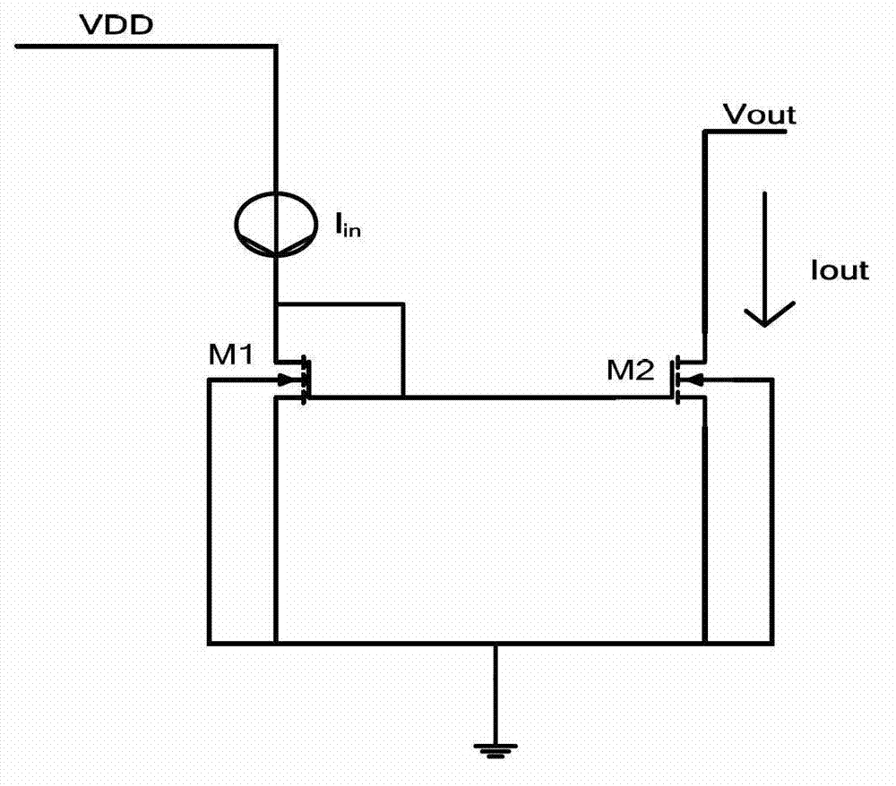
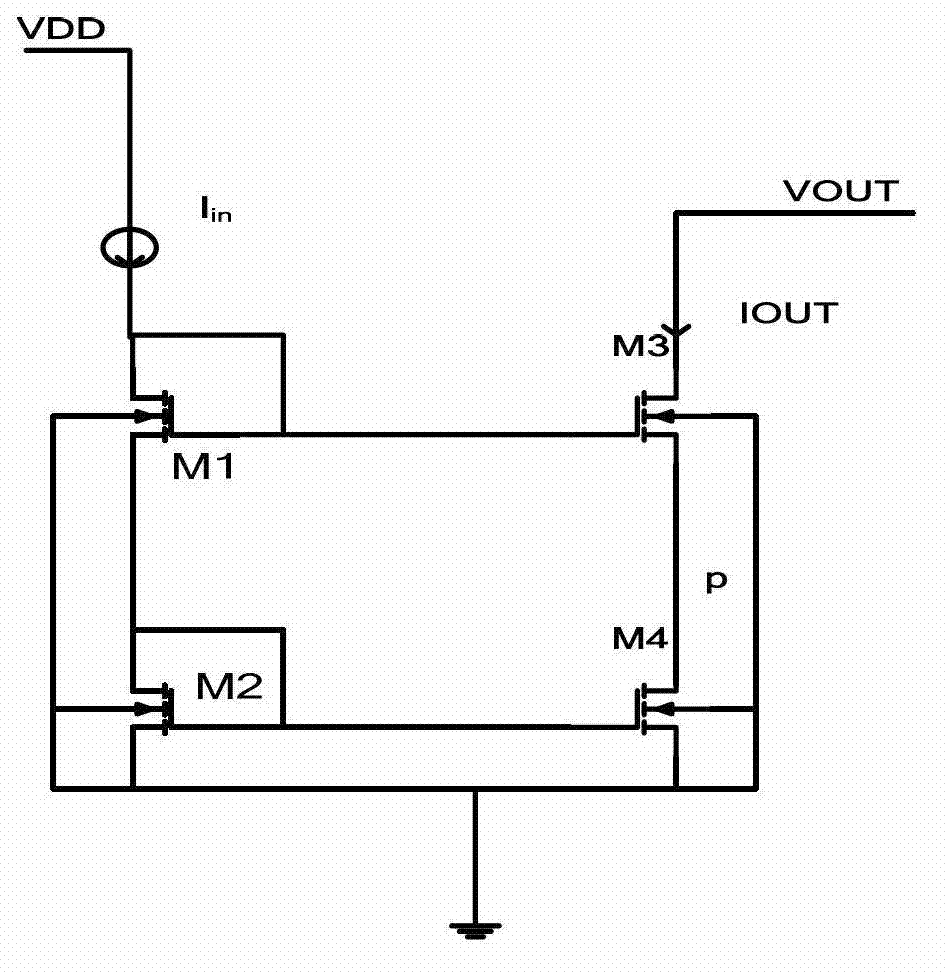
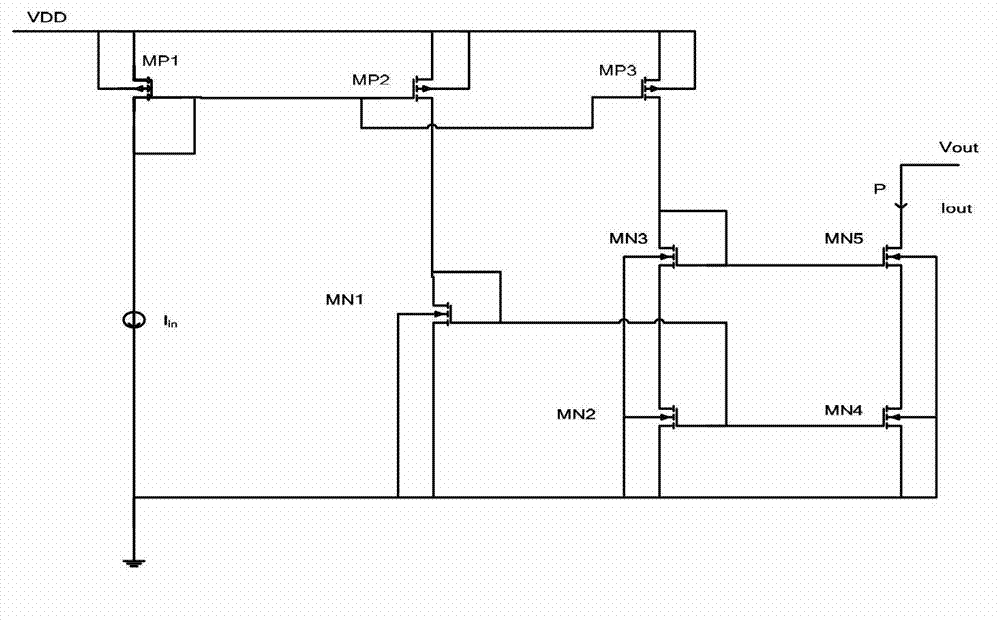
[0030] In order to balance the impact of mirror image accuracy and voltage margin on the circuit and meet low-voltage applications, without compromising circuit accuracy, reduce the voltage margin consumed by the circuit and increase the output swing of the circuit, making the design of the low-voltage current mirror necessary.

[0031] The present invention proposes a new low-voltage current mirror structure, which can reduce the voltage margin consumed by the circuit while ensuring the accuracy of the current mirror, improve the output voltage swing of the circuit, and reduce the influence of the load on the output current. This circuit is espe...


PUM


Abstract

The invention discloses a low voltage current mirror, and aims to solve the problem that output voltage swing is reduced because threshold voltage is wasted by the voltage redundancy of the conventional cascode current mirror. The low voltage current mirror comprises an input current source, a first P-channel metal oxide semiconductor (PMOS) tube, a second PMOS tube, a third PMOS tube, a first N-channel metal oxide semiconductor (NMOS) tube, a second NMOS tube, a third NMOS tube, a fourth NMOS tube and a fifth NMOS tube. The low voltage current mirror has a cascode output structure, output resistance is very high, and the influence of a load on output current is relatively small, so that the mirror image precision of the current mirror is very high; and a channel length modulation effect is rationally used by the structure, so that compared with the cascode current mirror, the current mirror has the advantages that the redundancy of the threshold voltage is reduced, and the output voltage swing is increased.

Description

technical field [0001] The invention belongs to the field of electronic technology, and in particular relates to the design of a current mirror. Background technique [0002] The current mirror is an indispensable module in the analog circuit. It can be used as a bias unit or a signal processing unit, and its performance plays a very critical role in the realization of the entire circuit. [0003] figure 1 is a schematic diagram of an existing MOS current mirror, the input current source I in and NMOS transistors M1 and M2, where the input current source I in is generated by the reference current source in the circuit. figure 1 The basic principle is to ensure the gate-source voltage V of M1 and M2 tubes GS Consistent, ignoring the channel length modulation effect, so according to the I-V square law of the MOS tube: [0004] I D = 1 2 μ C ox ...

Claims


Application Information

Patent Timeline
Patent Type & Authority Applications(China)
IPC IPC(8): G05F3/26
Inventor 方健唐莉芳吴杰杨毓俊黎俐陶垠波潘福跃臧凯旋
Owner UNIV OF ELECTRONICS SCI & TECH OF CHINA
Why Eureka
Try Eureka