LED display microarray and preparation method thereof

An array and micro-display technology, applied in the direction of electrical components, electrical solid devices, circuits, etc., can solve the problems of great difficulty in implementation, and achieve the effect of reducing depth, cost, and process difficulty

Inactive Publication Date: 2012-12-12
BEIJING UNIV OF TECH
View PDF15 Cites 3 Cited by
  • Summary
  • Abstract
  • Description
  • Claims
  • Application Information

AI Technical Summary

Problems solved by technology

However, the key technology in the manufacture of LED micro-display devices lies in the manufacture of isolation trenches. The invention patent No. ZL200720093946.2 proposes to use ICP technology to etch the upper and lower isolation trenches to realize the division of the LED light-emitting layer and the light-transmitting layer. This method has many problems. It is difficult to implement and has not been applied to the actual production field

Method used


Image

  • LED display microarray and preparation method thereof
  • LED display microarray and preparation method thereof
  • LED display microarray and preparation method thereof

Examples


Embodiment Construction

[0031] The direct light-emitting display array of the present invention will be described in detail below in conjunction with the accompanying drawings:

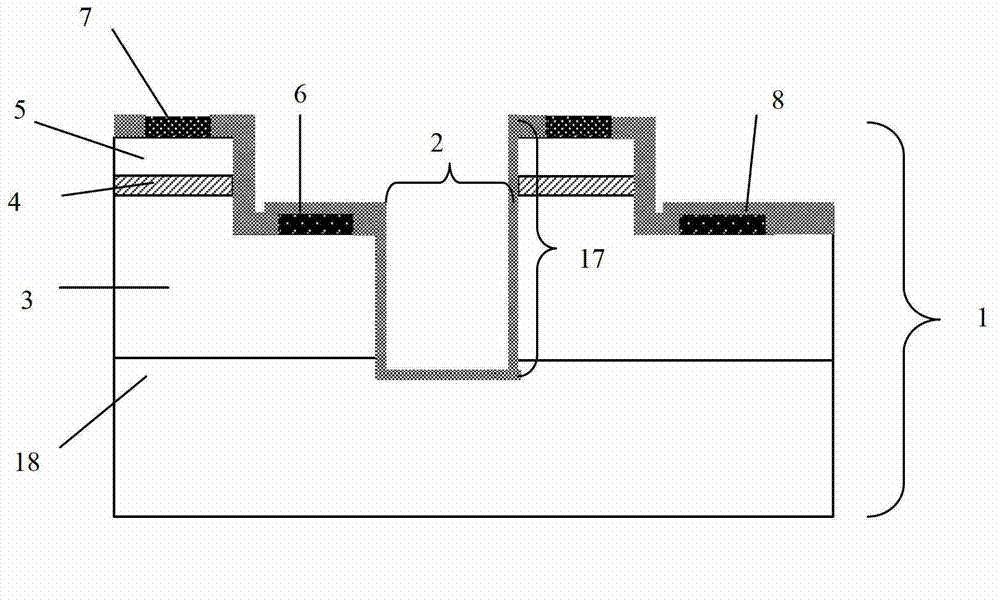
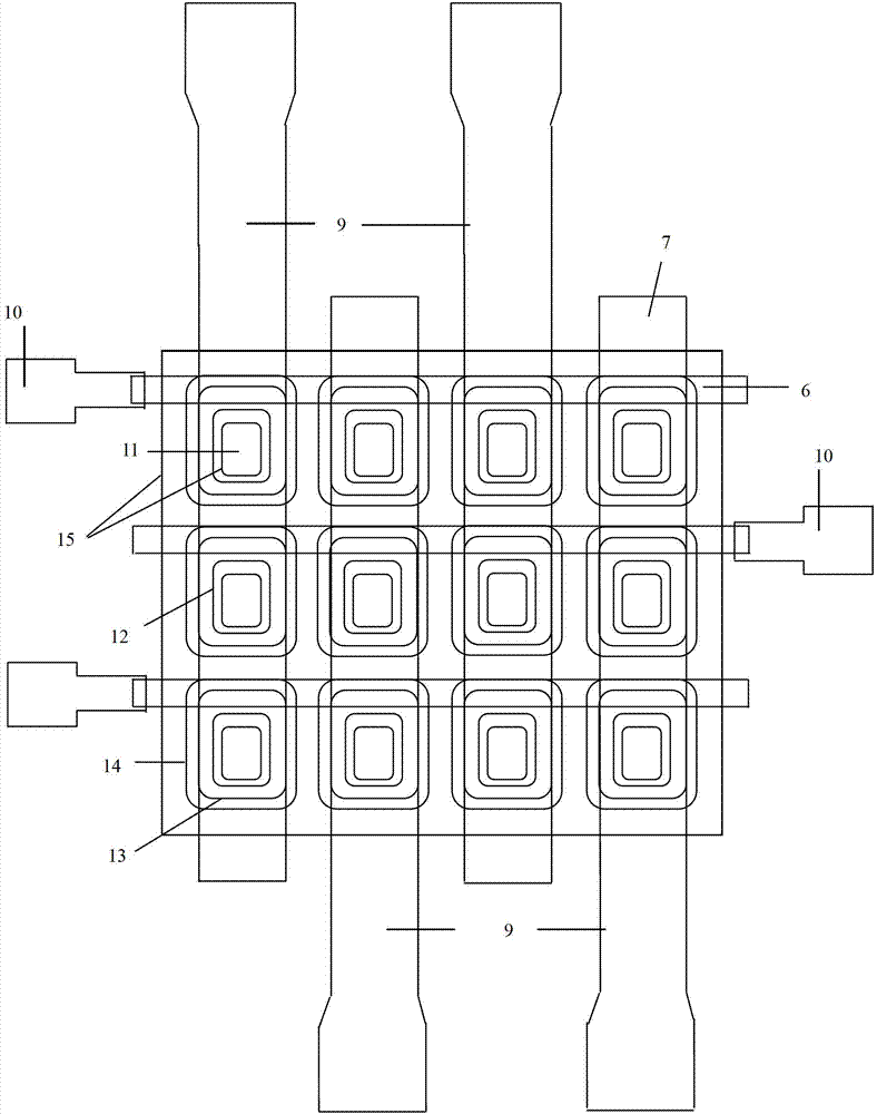
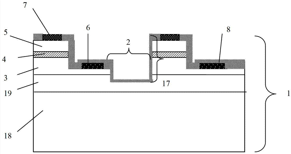
[0032] Such as Figures 3 to 5 As shown, an LED micro-display array of the present invention is characterized in that it includes an epitaxial wafer 1, a semiconductor matrix unit 17, a semiconductor matrix isolation region 2, an n-type conductive layer 3, a light-emitting layer 4, a p-type conductive layer 5, and an n-electrode 6 , p-electrode 7, isolation protective layer 8, anode line 9, cathode line 10; the epitaxial wafer 1 includes a substrate 18, and an insertion layer 19, an n-type conductive layer 3, and a light-emitting layer grown sequentially on the substrate 18 4 and the p-type conductive layer 5; on the horizontal and vertical strips of the epitaxial wafer 1, a dry etching method is used to etch part of the n-type conductive layer 3, and the strips are etching strips, The part between the etching strips consti...


PUM


Abstract

The invention relates to an LED display microarray and a preparation method thereof and belongs to the technical field of semiconductor illumination. The LED display microarray comprises a substrate epitaxial wafer, a semiconductor matrix isolation region, an insertion layer, an electronic conducting layer, a light-emitting layer, a hole conducting layer, an electronic conducting electrode, a hole conducting electrode, an isolation protecting layer, anode lines and cathode lines. An epitaxial layer is subjected to dry etching so that the electronic conducting layer and a semiconductor matrix cell array are obtained; the electronic conducting layer to the insertion layer is subjected to dry etching so that isolation of each two adjacent cells is achieved, and the semiconductor matrix isolation region is obtained; the electronic conducting electrode is formed to lead the cathode lines out; the isolation protecting layer is deposited; the hole conducting electrode is formed to lead the anode lines out; and the spatially intersectional regions of the anode lines and the cathode lines are display pixels. By the LED display microarray and the preparation method, the insertion layer is grown epitaxially to achieve isolation, the problem of electricity leakage caused by process difficulty in achievement of deep isolation trenches by a dry etching method is reduced, the depth of isolation trenches is decreased, and cost is lowered.

Description

technical field [0001] The invention belongs to the field of semiconductor lighting, and in particular relates to an LED display microarray and a preparation method thereof. technical background [0002] With the rapid development of electronic products and mobile communications, research on micro-display devices is booming. The progress of science and technology and society has given people a more colorful world. At the same time, people's requirements for display devices are also increasing. Light-emitting diodes (LEDs) have the advantages of being all solid and high luminous efficiency, and have been widely used in the field of display and lighting, and display technology has also emerged as a result. However, the key technology in the manufacture of LED micro-display devices lies in the manufacture of isolation trenches. The invention patent No. ZL200720093946.2 proposes to use ICP technology to etch the upper and lower isolation trenches to realize the division of the ...

Claims


Application Information

Patent Timeline
Patent Type & Authority Applications(China)
IPC IPC(8): H01L27/15H01L33/00
Inventor 郭伟玲丁艳朱彦旭刘建朋
Owner BEIJING UNIV OF TECH
Why Eureka
Try Eureka