Memory element and memory device

A storage element and storage layer technology, applied in electrical components, information storage, static memory, etc., can solve the problems of insufficient improvement of retention characteristics and repeat operation characteristics, and achieve the effect of improving repeat operation characteristics

Active Publication Date: 2012-12-12
SONY CORP
View PDF9 Cites 3 Cited by
  • Summary
  • Abstract
  • Description
  • Claims
  • Application Information

AI Technical Summary

Problems solved by technology

However, such memory elements have not sufficiently improved retention characteristics and repeated operation characteristics, and further improvement of these characteristics has been desired

Method used


Image

  • Memory element and memory device
  • Memory element and memory device
  • Memory element and memory device

Examples


Embodiment approach

[0036] 1. Memory element: a memory element with a single-layer structure in which the variable resistance layer is

[0037] 2. Storage device

[0038] [Modification]

[0039] (The variable resistance layer is a memory element with a multilayer structure)

Embodiment

[0041] [implementation mode]

[0042] [storage element]

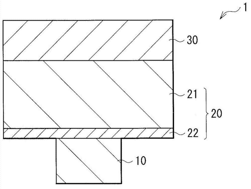
[0043] figure 1 It is a cross-sectional view showing the structure of the memory element 1 according to the embodiment of the present invention. This memory element 1 is configured to include a memory layer 20 provided between a lower electrode 10 (first electrode) and an upper electrode 30 (second electrode).

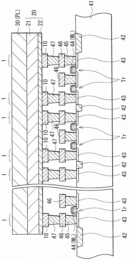
[0044] For example, the lower electrode 10 is provided on the substrate 41, and the substrate 41 is provided with ( figure 2 ) CMOS (Complementary Metal Oxide Semiconductor) circuit, so that the lower electrode 10 serves as a connection portion with the CMOS circuit. This lower electrode 10 is made of the following wiring materials used in semiconductor processes, such as W (tungsten), WN (tungsten nitride), TiN (titanium nitride), Cu (copper), Al (aluminum), Mo ( Molybdenum), Ta (tantalum) and silicide. When the lower electrode 10 is made of a material such as copper that may cause ion conduction in an elec...


PUM


Abstract

A memory element and a memory device comprising the same are disclosed. The memory element includes: a memory layer disposed between a first electrode and a second electrode. The memory layer includes: an ion source layer containing one or more metallic elements, and one or more chalcogen elements of tellurium (Te), sulfur (S), and selenium (Se); and a resistance change layer disposed between the ion source layer and the first electrode, the resistance change layer including a layer which includes tellurium and nitrogen (N) and is in contact with the ion source layer. The retention characteristics of the memory element and the memory device in the invention are maintained satisfactorily and the repetitive operation characteristics are improved.

Description

[0001] Cross References to Related Applications [0002] This application contains subject matter related to and claims priority from Japanese Patent Application JP2011-129769 filed in the Japan Patent Office on Jun. 10, 2011, the entire content of which is hereby incorporated by reference. technical field [0003] The present invention relates to a memory element that stores information based on changes in electrical characteristics of a memory layer including an ion source layer and a resistance change layer, and a memory device. Background technique [0004] Conventionally, as a nonvolatile memory from which information is not erased even if the power is turned off, flash memory, FeRAM (Ferroelectric Random Access Memory), MRAM (Magnetoresistive Random Access Memory), and the like have been proposed. These types of memory can hold written information for long periods of time without power. However, each of these memories has advantages and disadvantages. That is, flash ...

Claims


Application Information

Patent Timeline
Patent Type & Authority Applications(China)
IPC IPC(8): H01L45/00
CPCG11C2213/56H01L45/1266H01L27/2472H01L45/1233H01L45/1641H01L45/145H01L45/00H01L27/2436G11C11/00H01L45/144H01L45/146H01L45/085G11C11/5614G11C13/0011G11C13/00H01L45/08H10B63/82H10B63/30H10N70/24H10N70/245H10N70/8416H10N70/883H10N70/041H10N70/8828H10N70/826H10N70/8833H10N70/8822H10N70/8825
Inventor 水口彻也保田周一郎紫牟田雅之大场和博荒谷胜久
Owner SONY CORP
Why Eureka
Try Eureka