Resistance change memory device and method of operating resistance change memory device

A resistance-variable, storage device technology, applied in static memory, read-only memory, electric solid state devices, etc., can solve the problems of low repetition characteristics, difficulty in resistance, increase, etc., and achieve the effect of improving high-speed operation

Inactive Publication Date: 2016-11-23
SONY SEMICON SOLUTIONS CORP
View PDF9 Cites 0 Cited by
  • Summary
  • Abstract
  • Description
  • Claims
  • Application Information

AI Technical Summary

Problems solved by technology

[0012] However, ReRAM also has the disadvantage that it is difficult to obtain a desired resistance value when the accuracy of current control is low, and in particular, excessive application of current makes it difficult to perform resistance increase (reset) operation, or leads to poor repetition characteristics
Therefore, it is difficult to suddenly change the potential of the bit line
Therefore, since the wiring capacitance of the bit line is smaller than that of the word line, the operating speed that should normally be high may not be high enough

Method used


Image

  • Resistance change memory device and method of operating resistance change memory device
  • Resistance change memory device and method of operating resistance change memory device
  • Resistance change memory device and method of operating resistance change memory device

Examples


no. 1 example

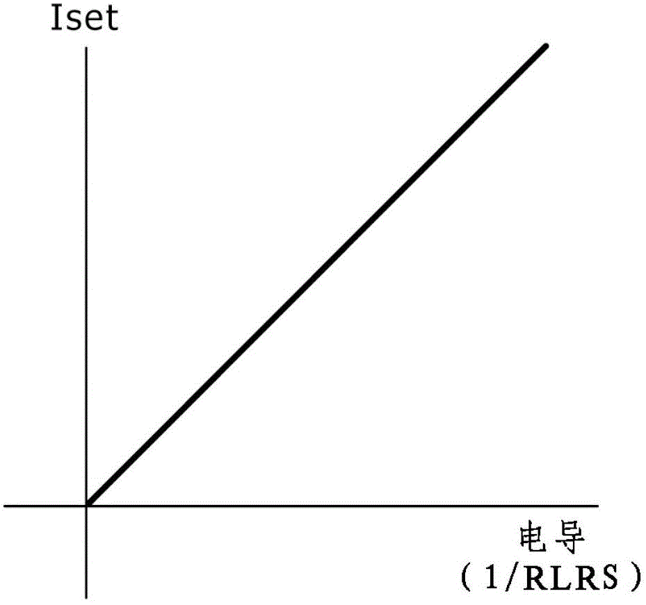
[0045] 1. First Embodiment: A case in which a current is drawn from the bit line by starting the operation of reducing the resistance by lowering the potential of the bit line. A configuration is disclosed in which, at the start of the operation for reducing the resistance, the current flowing through the bit line is switched from the first current to the second current by using two transistors connected in parallel with each other.

no. 2 example

[0046] 2. Second Embodiment: When the bit line current is drawn out similarly to the case of the first embodiment, the switching of the current is performed by using one transistor.

no. 3 example

[0047] 3. Third Embodiment: The operation for reducing the resistance is started by raising the potential of the bit line, thereby applying a current to the bit line.

[0048] 4. Fourth Embodiment: A case where a P-channel transistor is used as an access transistor.

[0049] 5. Variations

[0050] 1. First Embodiment

[0051] The composition of the storage unit

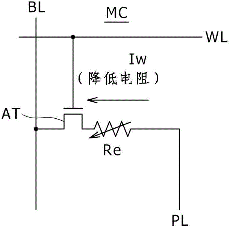
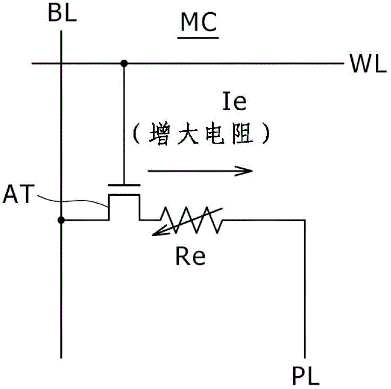
[0052] Figure 2A and Figure 2B Equivalent circuit diagrams of memory cells common to the embodiments of the present invention are respectively shown. It should be noted that although Figure 2A shows the direction of the write current, Figure 2B shows the direction of the erase current, but for Figure 2A and Figure 2B , the memory cell structure itself is the same.

[0053] Figure 2A and Figure 2B The memory cell MC shown in includes one variable resistance element Re and one access transistor AT as "memory elements".

[0054] One end of the variable resistance element Re is connected to the plate P...


PUM


Abstract

The invention discloses a resistance variable memory device and an operation method thereof. The variable resistance memory device includes: a bit line; a voltage supply layer; a memory element connected between the bit line and the voltage supply layer, the resistance value of the memory element changing according to an applied voltage. change; and a drive control circuit that causes a first current to flow through the bit line and a second current smaller than the first current to flow through the bit line, whereby by using the second current to A resistance lowering operation that causes the memory element to change from a high resistance state to a low resistance state is controlled. The operating method includes the steps of: flowing a first current through a bit line during the resistance lowering operation; and flowing a second current smaller than the first current through the bit line, thereby controlling all of the memory elements. The resistance reduction operation described above. According to the present invention, current control of bit lines can be performed with improved high-speed performance.

Description

[0001] CROSS-REFERENCE TO RELATED APPLICATIONS [0002] The present application contains subject matter related to that disclosed in Japanese Priority Patent Application JP 2011-132576 filed in the Japan Patent Office on Jun. 14, 2011, the entire content of which is hereby incorporated by reference. technical field [0003] The present invention relates to a resistance change memory device in which a memory element whose resistance value changes according to an applied voltage is connected between a bit line and a source line, and to a method of operating the resistance change memory device. It is alternately connected between the bit line and a voltage supply layer called a "plate". Background technique [0004] A resistance change-type memory device is known in which the resistance value of a memory element of each memory cell is changed by implanting conductive ions into an insulating film or extracting conductive ions from the insulating film. For example, in the non-pa...

Claims


Application Information

Patent Timeline
Patent Type & Authority Patents(China)
IPC IPC(8): G11C11/56
CPCG11C13/0002G11C13/0026G11C13/0069G11C2013/0092G11C2213/79H10B63/30H10N70/245H10N70/8416H10N70/826H10N70/883G11C13/00G11C16/06
Inventor 北川真
Owner SONY SEMICON SOLUTIONS CORP
Why Eureka
Try Eureka