

Consumable chip, consumable container and data writing method for the consumable chip
Patent Information
- Authority / Receiving Office
- CN · China
- Patent Type
- Patents(China)
- Current Assignee / Owner
- ZHUHAI TIANWEI TECH DEV CO LTD
- Publication Date
- 2015-02-25
Smart Images
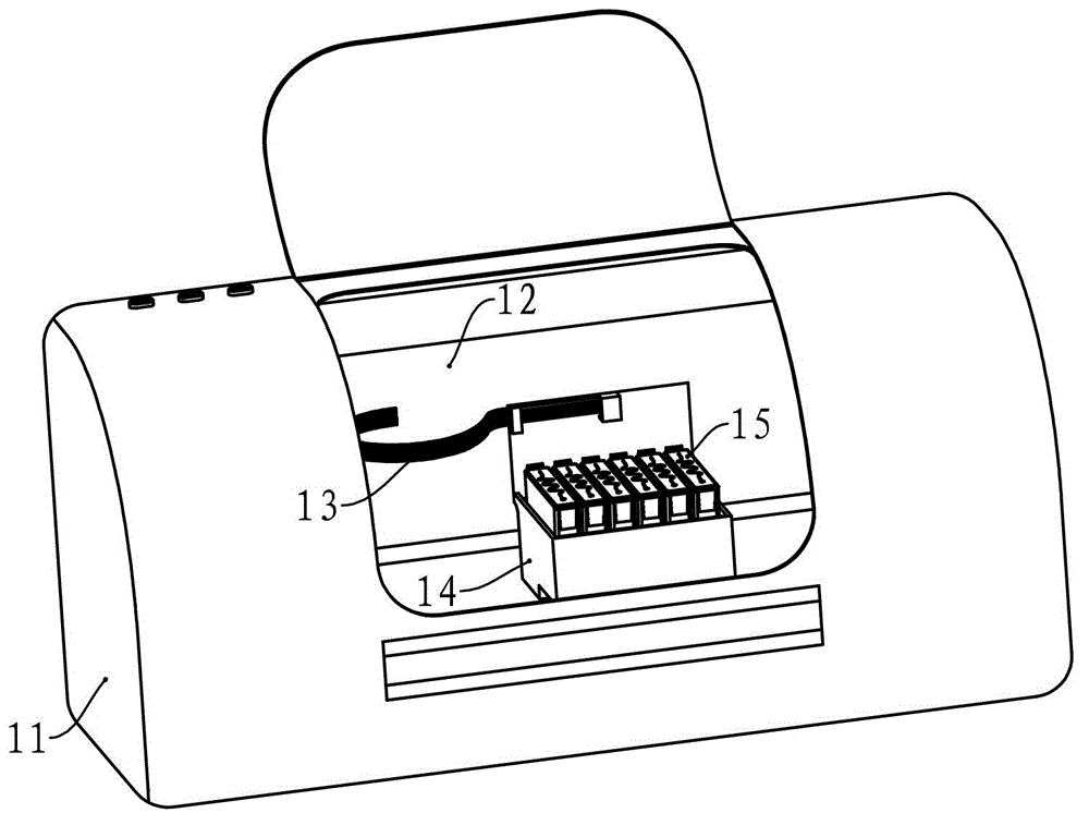
Figure 1 
Figure 2 
Figure 3
Abstract
Description
technical field
[0001] The invention relates to the field of printing consumables, in particular to a consumable chip, a consumable container with the chip, and a data writing method for the consumable chip. Background technique
[0002] As a common office equipment, printers provide great convenience for modern office. Existing printers are divided into inkjet printers and laser printers. Inkjet printers use ink cartridges containing ink as consumable containers to spray ink on paper to form text or patterns that need to be printed on paper; laser printers use ink cartridges containing toner The toner cartridge is used as a consumable container to form text or patterns that need to be printed on the medium.
[0003] see figure 1 , an existing color inkjet printer has a casing 11, figure 1 The inkjet printer is shown with the chassis 11 omitted. The machine core 12 of ink-jet printer is provided with in the casing 11, and is provided with a slide bar, print word car 14 i...