Semiconductor device manufacturing device and semiconductor device manufacturing method

A technology for manufacturing devices and manufacturing methods, applied in semiconductor/solid-state device manufacturing, semiconductor devices, electric solid-state devices, etc., can solve problems such as semiconductor chip damage and semiconductor chip surface damage, and achieve the effect of reducing incompleteness and damage

Inactive Publication Date: 2015-09-30
FUJI ELECTRIC CO LTD
View PDF7 Cites 0 Cited by
  • Summary
  • Abstract
  • Description
  • Claims
  • Application Information

AI Technical Summary

Problems solved by technology

However, when such a pick-up method is applied to a thinned semiconductor chip, the surface of the semiconductor chip may be damaged or the semiconductor chip may be damaged by pushing up the semiconductor chip with a needle or the like.

Method used


Image

  • Semiconductor device manufacturing device and semiconductor device manufacturing method
  • Semiconductor device manufacturing device and semiconductor device manufacturing method
  • Semiconductor device manufacturing device and semiconductor device manufacturing method

Examples


Embodiment approach 1

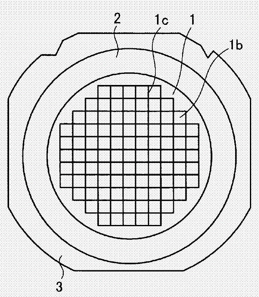
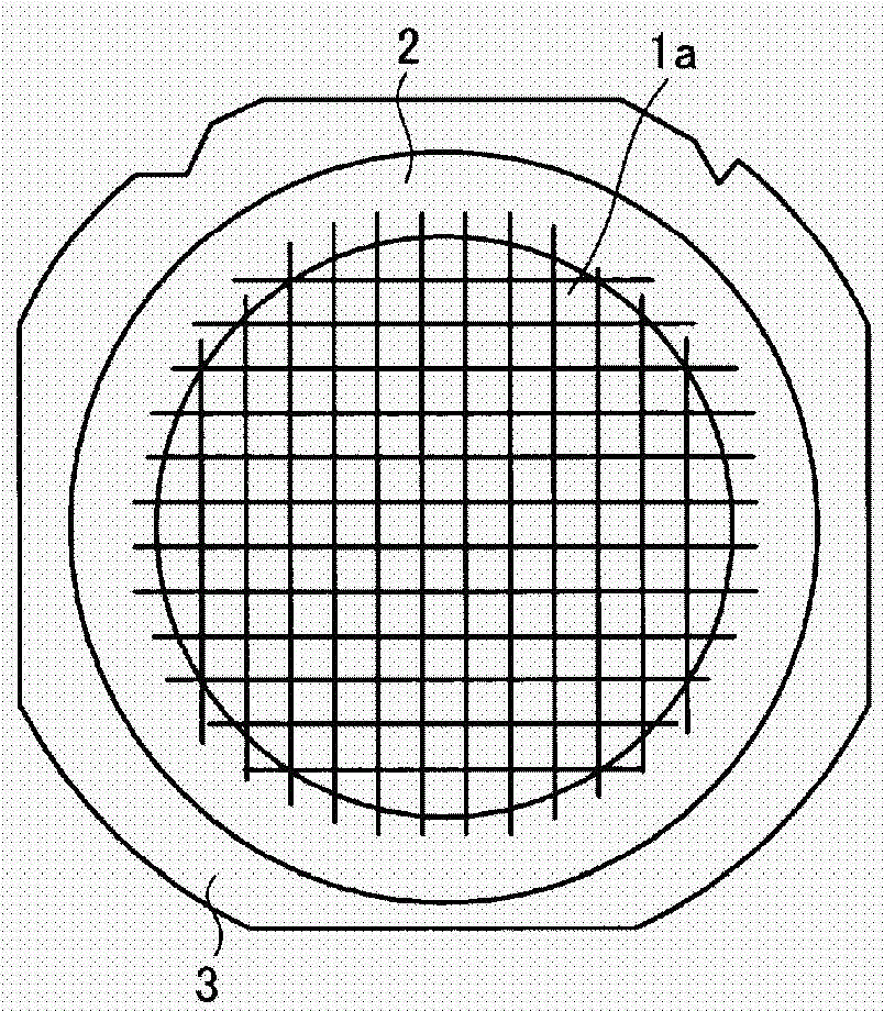
[0071] figure 1 It is a plan view showing a semiconductor wafer processed in the semiconductor device manufacturing apparatus of the first embodiment. figure 2 yes means figure 1 A plan view of the diced state of the semiconductor wafer is shown. The semiconductor wafer 1 before being processed in the semiconductor device manufacturing apparatus of the first embodiment will be described. Such as figure 1 , 2 As shown, a semiconductor wafer 1 is diced with a tape (dicing tape) 2 attached thereto, and is cut into individual semiconductor chips 1 a on which a device surface structure (electronic circuit) is formed.

[0072] Specifically, the semiconductor wafer 1 is cut into individual semiconductor chips 1a by dicing, for example, as follows. First, if figure 1 As shown, in each formation region 1 b of the semiconductor chip, the surface structure of the device is formed on the surface side of the semiconductor wafer 1 . The formation regions 1b of the semiconductor ...

no. 2 approach )

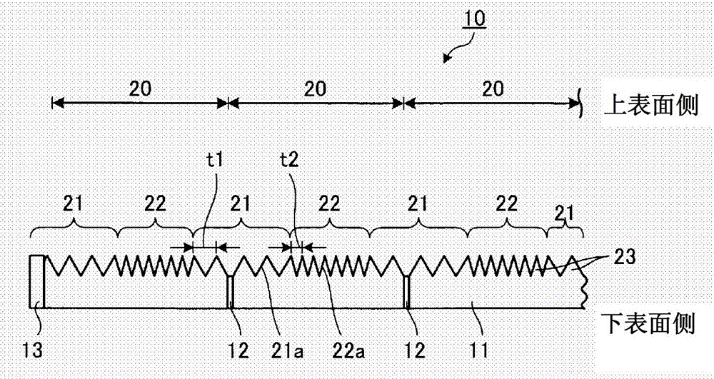
[0113] Figure 11 It is a cross-sectional view showing main parts of the semiconductor device manufacturing apparatus of the second embodiment. in addition, Figure 12 It is a cross-sectional view showing a semiconductor chip held in the semiconductor device manufacturing apparatus of the second embodiment. The semiconductor device manufacturing apparatus (pickup apparatus) 40 of the second embodiment differs from the semiconductor device manufacturing apparatus of the first embodiment in that the cross-sectional shapes of the first groove 51 a and the second groove 52 a are rectangular.

[0114] Such as Figure 11 As shown, the holding table 11 of the pick-up device 40 has: a first groove 51a and a second groove 52a arranged on the upper surface of the holding table 11; at least one air hole connected with the first groove 51a and the second groove 52a 12 ; and the outer wall portion 13 that contacts the side surface of the holding table 11 and surrounds the holding table ...


PUM


Abstract

The present invention provides a semiconductor device manufacturing apparatus and a semiconductor device manufacturing method which are capable of reducing incompleteness and damages of semiconductor chips when being peeled off from a rubber belt. A pickup apparatus (10) is provided with a semiconductor chip maintenance table (11) for maintaining the semiconductor chip to be stuck on the rubber belt, and a first groove (21a) and a second groove (22a) disposed on the side, where the semiconductor chips are maintained, of the maintenance table (11), wherein the first groove (21a) and the second groove (22a) are connected with at least two air vents (12), and the width (t2) of an opening portion of the second groove is smaller than the width (t1) of the opening portion of the first groove. The semiconductor chip is maintained on peak parts of the first and the second grooves in a manner that the side stuck with the rubber belt faces downwards, a pressure-reducing mechanism is used to reduce pressure in an enclosed space enclosed by the rubber belt, the first groove and the second groove, and then the pickup apparatus (10) picks up the semiconductor chip from the maintenance table by using a chunk.

Description

technical field [0001] The present invention relates to a semiconductor device manufacturing device and a semiconductor device manufacturing method. Background technique [0002] In recent years, in IGBT (Insulated Gate Bipolar Transistor: Insulated Gate Bipolar Transistor), in order to achieve high performance and low cost, the thickness of semiconductor wafers has been reduced. For example, a technique for reducing the thickness of a semiconductor wafer to about 50 μm to 100 μm or less has been proposed. [0003] In manufacturing a thin semiconductor device, for example, after forming a device structure on the surface of a semiconductor wafer, back grinding and / or silicon etching are performed on the back surface of the semiconductor wafer to achieve a predetermined thickness. Then, dicing is performed for each device structure formed on the surface of the semiconductor wafer, and the semiconductor wafer is cut into individual semiconductor chips. [0004] In addition, t...

Claims


Application Information

Patent Timeline
Patent Type & Authority Patents(China)
IPC IPC(8): H01L21/683
CPCH01L2224/83385
Inventor 田中阳子
Owner FUJI ELECTRIC CO LTD
Why Eureka
Try Eureka