Object surface defect detection method and apparatus based on linear array CCD

A technology for defect detection and object surface, which is applied in the direction of optical detection of defects/defects, etc., can solve the problems of high detection accuracy, achieve high detection accuracy, easy correction of distortion errors, and simple structure

Inactive Publication Date: 2013-01-02
CENT SOUTH UNIV
View PDF5 Cites 22 Cited by
  • Summary
  • Abstract
  • Description
  • Claims
  • Application Information

AI Technical Summary

Problems solved by technology

[0010] The technical problem to be solved by the present invention is to provide a method and device for detecting surface defects of objects based on linear array CCD. The method and device for detecting surface defects of objects based on linear array CCD have fast detection speed, high detection accuracy, and simple structure. Low cost, suitable for online detection of a single defect on the surface image of an object on the production line

Method used


Image

  • Object surface defect detection method and apparatus based on linear array CCD
  • Object surface defect detection method and apparatus based on linear array CCD
  • Object surface defect detection method and apparatus based on linear array CCD

Examples


Embodiment 1

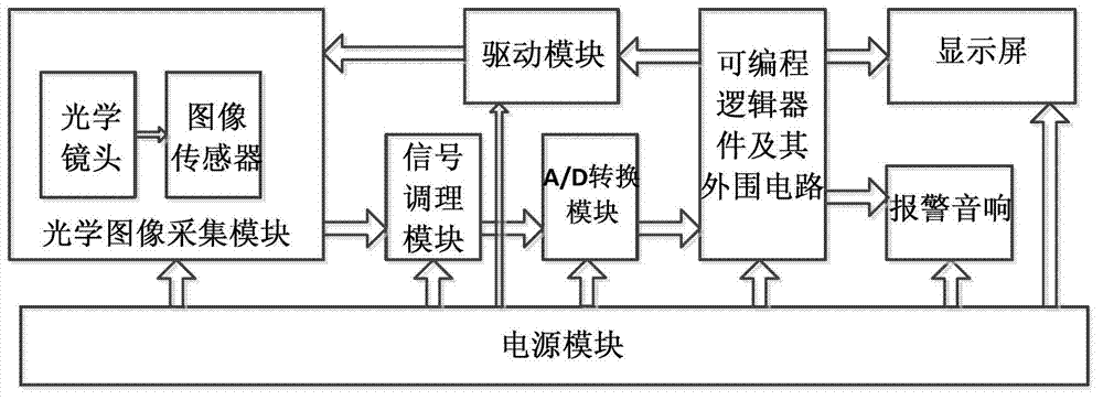
[0058] see figure 1 , the invention includes an optical image acquisition module, a signal conditioning module, an A / D conversion module, a driving module, a power supply module, a programmable logic device and peripheral circuits thereof. The programmable logic device is the core of the system, and is respectively connected with the A / D conversion module, the driving module, the power supply module and the like.

[0059] Optical image acquisition module. The module consists of a light source, an optical lens and an image sensor, and is responsible for collecting images of the surface of the object. The image sensor uses a linear array CCD. The module is powered by the power module and driven by the driver module, and the image information of the surface of the object collected by it is sent to the signal conditioning module.

[0060] Signal Conditioning Module. The module includes two parts of amplification and filtering, which is the prior art. Since the output analog s...

specific example

[0068] A specific example is as follows:

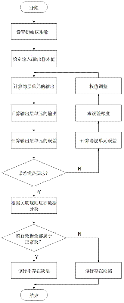
[0069] 1. The learning stage. Before classifying the data, there is a self-learning phase. In this stage, the BP neural network algorithm is used to extract the surface features of the material. Proceed as follows:

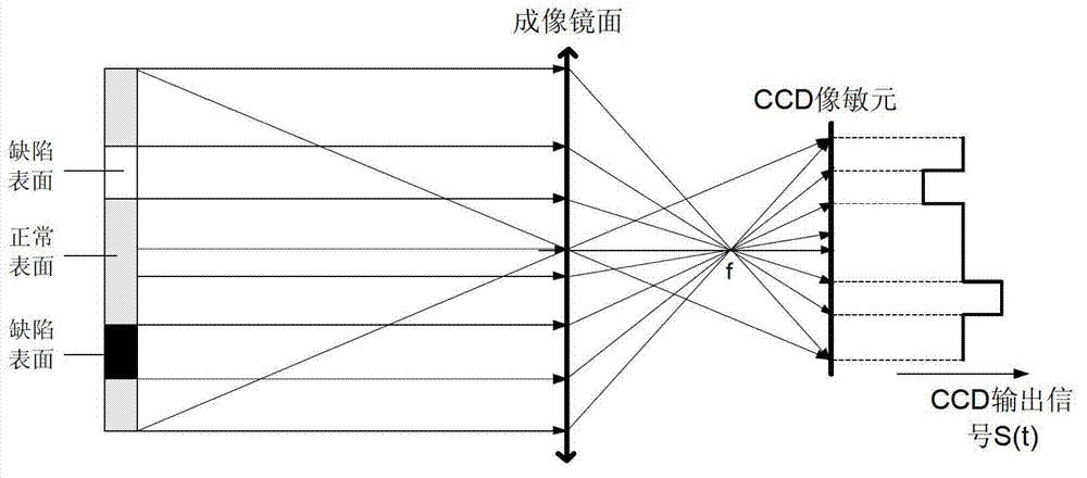
[0070] 1), data preprocessing. Before starting the training, it is necessary to normalize the collected sample data and re-encode the discrete data category attributes. First divide the corresponding voltage value in the sample by the maximum attribute value of the column, so that its input value is limited to the interval [0,1]. For discrete data category attributes, recode, and use 0 to represent "defect". Use 1 for "normal", as expected output. The normalized data is shown in Table 2. [The output voltage of the CCD is the output voltage of each pixel. Although the size of a defect is generally unlikely to be as large as one pixel, our solution is to use the method of judging whether there is a defect line by line...


PUM


Abstract

The invention discloses an object surface defect detection method and an object surface defect detection apparatus based on a linear array CCD. According to the apparatus, the image information of surfaces of the objects on a production line is collected by using a fixed linear array CCD; defect identification and defect location determination are carried out by using a method of non-interlaced defect detection with a BP neural network algorithm according to the collected image information. The apparatus comprises an optical image collection module, a signal conditioning module, an A/D conversion module, a driving module, a power supply module, and a programmable logic device and peripheral circuits and a software system thereof. The programmable logic device is the core of the apparatus. The method and the apparatus provided by the invention have the advantages of high detection speed, high detection accuracy, simple structure, and low cost. The method and the apparatus are suitable to be used in single defect detections upon surface images of objects on the production line.

Description

technical field [0001] The invention relates to an object surface defect detection method and device based on a linear array CCD. Background technique [0002] In the materials and material products of many industries, surface defects are one of the important factors affecting product quality. For example, defects such as scarring and pitting of steel plates, aluminum plates, and copper foils not only affect the appearance of the product, but more seriously reduce the quality of the product. The corrosion resistance, wear resistance and fatigue strength of the product are improved; in addition, in the application field of high-quality polymer films, the defects of film materials will also affect the performance of products, for example, for large-screen flat panel displays, the defects of film materials will affect The electrical insulation performance of the protective screen; for high-quality packaging materials, the defects of the film material will reduce the heat resist...

Claims


Application Information

Patent Timeline
Patent Type & Authority Applications(China)
IPC IPC(8): G01N21/88
Inventor 邹润民王勋志郭述帆
Owner CENT SOUTH UNIV
Why Eureka
Try Eureka