Liquid crystal display panel and repairing method thereof

A liquid crystal display panel and panel technology, applied in nonlinear optics, instruments, optics, etc., can solve the problems of occupying substrate wiring space, electrostatic damage, and increased metal crossing overlapping positions, and achieve the effect of saving wiring space

Inactive Publication Date: 2013-01-02
NANJING CEC PANDA LCD TECH
View PDF2 Cites 23 Cited by
  • Summary
  • Abstract
  • Description
  • Claims
  • Application Information

AI Technical Summary

Problems solved by technology

Because multiple sets of data test lines of the test circuit and multiple repair lines of the line repair circuit are respectively arranged on the periphery of the substrate, this occupies a large wiring space around the substrate
At the same time, it will increase the overlapping positions of metal crossings of different layers around the substrate, which is prone to electrostatic damage, thus destroying the wiring

Method used


Image

  • Liquid crystal display panel and repairing method thereof
  • Liquid crystal display panel and repairing method thereof
  • Liquid crystal display panel and repairing method thereof

Examples


Embodiment Construction

[0039] In the following, the present invention will be further clarified with reference to the accompanying drawings and specific embodiments. It should be understood that these embodiments are only used to illustrate the present invention and not to limit the scope of the present invention. After reading the present invention, those skilled in the art will understand various aspects of the present invention. Modifications in equivalent forms fall within the scope defined by the appended claims of this application.

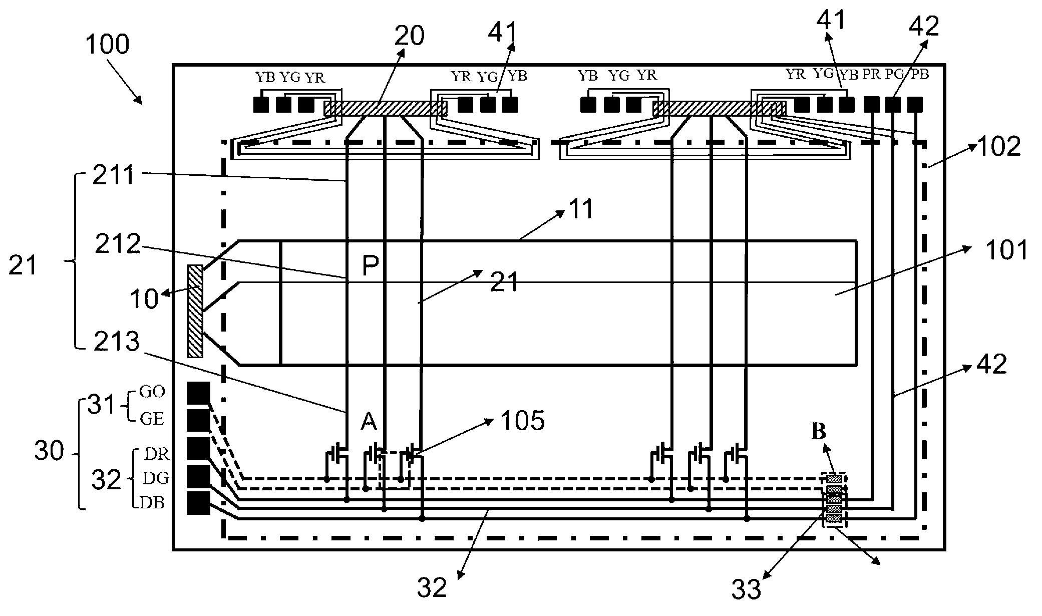
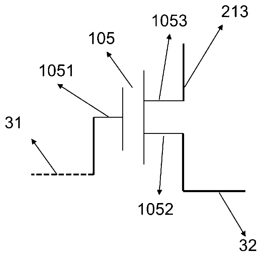
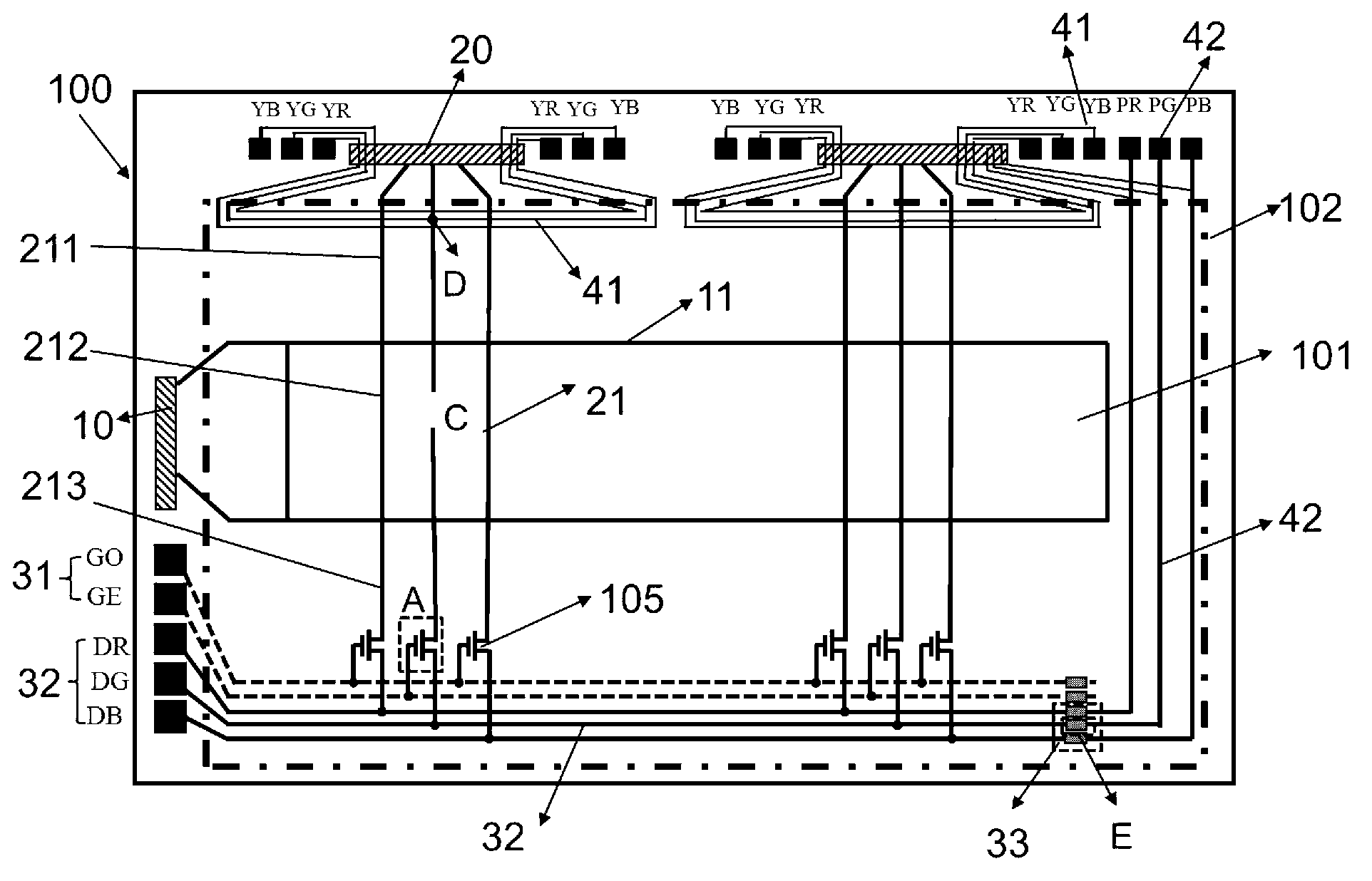
[0040] figure 1 It is a schematic diagram of testing the liquid crystal panel of the present invention. The liquid crystal panel 100 includes a display area 101, a signal line arrangement area 102 located outside the display area 101, and a thin film transistor (TFT) 105 located outside the display area 101. A plurality of source drivers 20 and a plurality of gate drivers 10 are provided in the signal line arrangement area 102, and a plurality of data lines 21 and a p...


PUM


Abstract

The invention discloses a liquid crystal display panel and a repairing method of the liquid crystal display panel. The liquid crystal display panel comprises a data wire, a scanning line crossed with the data wire, a testing subassembly positioned in a signal wire setting area, and a repairing wire subassembly positioned in the signal wire setting area, wherein the repair wire subassembly comprises a first repairing wire set and a second repairing wire set, when the repairing is not performed, the first repairing wire set is separated from the corresponding front end data wire; the second repairing wire set is separated from the corresponding testing data wire; when the repairing is performed, the first repairing wire set is electrically connected with the corresponding front end data wire; and the second repairing wire set is electrically connected with the corresponding testing data wire. With the adoption of the technical scheme, the same routing is effectively utilized; a static protective circuit is adopted, therefore, the static protection function is achieved, and a wire repairing validating loop is added for timely validating.

Description

Technical field [0001] The invention relates to a liquid crystal display panel and a repair method thereof. Background technique [0002] The existing thin film transistor liquid crystal display panel includes a thin film transistor array substrate, a color filter substrate, and a liquid crystal layer sandwiched between two electrode plates. A large number of scan lines, data lines, and pixel units defined by the scan lines and data lines are arranged on the thin film transistor array substrate. These densely arranged data lines are often disconnected, causing signals to be unable to transmit normally, thereby forming line defects. The method in the prior art is to form a test circuit and a wire repair circuit around the array substrate while manufacturing the array substrate. After the substrate is cut into multiple panels, a lighting test is performed. When a data line is broken during the test, the broken line is repaired through a line repair circuit. Because multiple sets...

Claims


Application Information

Patent Timeline
Patent Type & Authority Applications(China)
IPC IPC(8): G02F1/1362G02F1/1368G02F1/13
Inventor 周刘飞
Owner NANJING CEC PANDA LCD TECH
Why Eureka
Try Eureka