Shift register, gate drive circuit and display apparatus

A gate drive circuit and shift register technology, applied in static memory, digital memory information, instruments, etc., can solve the problems of reducing circuit reliability, increasing power consumption, and high cost, so as to avoid threshold voltage drift and reduce individual Number, the effect of reducing power consumption

Active Publication Date: 2013-01-02
BOE TECH GRP CO LTD +1
View PDF7 Cites 32 Cited by
  • Summary
  • Abstract
  • Description
  • Claims
  • Application Information

AI Technical Summary

Problems solved by technology

[0004] In the existing gate drive circuit, there are problems of complex circuit and high cost due to the large number of transistors in the circuit. For example, in a gate drive circuit, the shift register includes cascaded multi-stages, wherein , each stage includes a pull-up unit, a pull-down unit, a reset unit, and a hold unit. The hold unit is used to generate a hold signal. The function of the hold unit needs to be realized by more transistors, often only in the hold unit. Eight transistors are used to provide hold signals. Such a shift register structure is relatively complicated, which reduces the reliability of the circuit and increases power consumption.

Method used


Image

  • Shift register, gate drive circuit and display apparatus
  • Shift register, gate drive circuit and display apparatus
  • Shift register, gate drive circuit and display apparatus

Examples


Embodiment 1

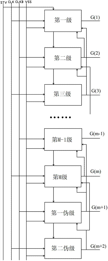
[0043] This embodiment describes a shift register, which is applied to a display substrate gate drive circuit. The shift register has cascaded M stages, and the Nth stage of the shift register includes:

[0044] The pull-up module outputs a driving signal to the output terminal of the Nth stage according to the input signal and the clock signal of the Nth stage;

[0045] A reset module, outputting a cutoff signal to the output terminal of the Nth stage according to the reset signal of the Nth stage;

[0046] The pull-down module maintains the output signal of the output terminal of the Nth stage as the cut-off signal according to the hold signal of the Nth stage;

[0047] Where N and M are natural numbers, and N is less than or equal to M;

[0048] When N is less than M-1, the hold signal of the Nth stage is the output signal of the output terminal of the N+2th stage;

[0049] The shift register also includes sequentially cascaded after the Mth stage:

[0050] The first dum...

Embodiment 2

[0053] This embodiment includes the whole content of embodiment one, but more specifically:

[0054] When N is 1, the input signal of the Nth stage is a field synchronization signal; when N is not 1, the input signal of the Nth stage is the output signal of the output terminal of the N-1th stage.

[0055] When N is less than M, the reset signal of the Nth stage is the output signal of the output terminal of the N+1th stage; when N=M, the reset signal of the Nth stage is the output signal of the first dummy stage.

[0056] In this embodiment, the first dummy stage and the second dummy stage can be reset by design methods such as using a vertical start pulse (STV) or an inverter.

[0057] In this embodiment, there is no need to use other signal generating devices, but the output signals of the upper stage and the lower stage are respectively used as the input signal, reset signal and hold signal of the current stage, which makes the circuit structure simpler.

Embodiment 3

[0059] This embodiment includes the whole content of embodiment two, but more specifically:

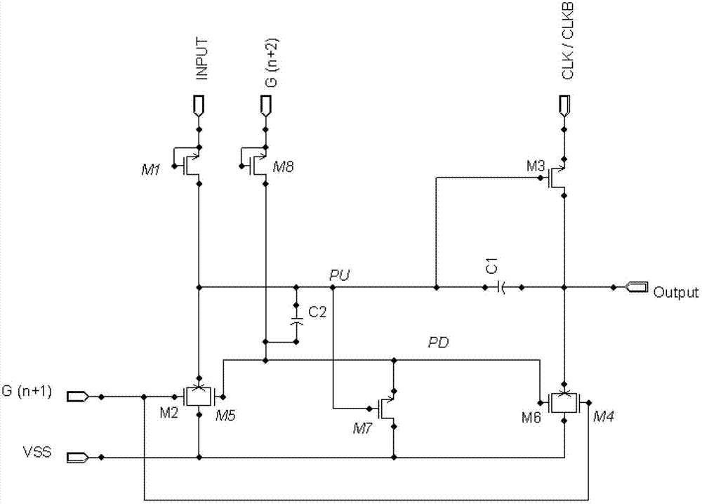
[0060] Such as figure 1 and figure 2 As shown, in this example:

[0061] The pull-up module includes a first transistor M1, a third transistor M3 and a first capacitor C1, wherein:

[0062] The gate and drain of the first transistor M1 (in the embodiment of the present invention, the source and drain of each transistor can be used interchangeably) are connected to the input signal, and the source is connected to the first node PU;

[0063]The gate of the third transistor M3 is connected to the first node PU, the drain is connected to the clock signal, and the source is connected to the output terminal Output;

[0064] The first capacitor C1 is connected between the first node PU and the output terminal Output.

[0065] The reset module includes a second transistor M2 and a fourth transistor M4, wherein:

[0066] The gate of the second transistor M2 is connected to the reset sign...


PUM


Abstract

The present invention discloses a shift register, which comprises a shift register, wherein the shift register has multiple levels, and the multiple levels are cascaded. The level N of the shift register comprises a pull-up module, wherein the pull-up module outputs a drive signal to an output terminal according to an input signal and a clock signal; a reset module, wherein the reset module outputs a cutoff signal to the output terminal according to a reset signal; and a drop-down module, wherein the drop-down module remains the output signal of the output terminal as the cutoff signal according to a retain signal, and a retain signal of the level N is an output signal of an output terminal of the level N+2. The present invention further discloses a gate drive circuit including the shift register and a display apparatus. According to the present invention, the liquid crystal display gate drive effect is achieved through the simple circuit structure, noise interference of the output terminal of the gate drive circuit is minimized, the number of thin film transistors in the pull-down module is reduced, and the purpose of power consumption reduction is achieved.

Description

technical field [0001] The invention relates to the field of display technology, in particular to a shift register, a gate drive circuit and a display device. Background technique [0002] The liquid crystal display panel adopts a progressive scan matrix display with M×N dot arrangement. The driver of Thin Film Transistor-Liquid Crystal Display (TFT-LCD) mainly includes a gate driver and a data driver, wherein the gate driver converts the input clock signal through a shift register and then adds it to the LCD panel on the grid. [0003] The shift register is often used in the gate driver of the liquid crystal display panel, and each gate line is connected with a stage circuit unit of the shift register. The gate-level input signal is output through the gate-level driving circuit, and each pixel is scanned row by row. The gate drive circuit can be installed in the display panel in the form of chip on flexible substrate technology (Chip on Flex, COF) or chip technology on g...

Claims


Application Information

Patent Timeline
Patent Type & Authority Applications(China)
IPC IPC(8): G11C19/28G09G3/36
Inventor 邵贤杰李小和
Owner BOE TECH GRP CO LTD
Why Eureka
Try Eureka