Supercharge Your Innovation With Domain-Expert AI Agents!

Interconnect barrier structure and method

A technology of barrier layer and compound barrier, which is applied in the field of interconnection barrier structure, can solve the problem of unsatisfactory top and bottom

Active Publication Date: 2013-01-02
TAIWAN SEMICON MFG CO LTD
View PDF5 Cites 8 Cited by
  • Summary
  • Abstract
  • Description
  • Claims
  • Application Information

AI Technical Summary

Problems solved by technology

This compromise between step coverage and resistance makes the barrier layer formed by CVD less than ideal for the top and bottom of the TSV

Method used


Image

  • Interconnect barrier structure and method
  • Interconnect barrier structure and method
  • Interconnect barrier structure and method

Examples


Embodiment Construction

[0040] The making and using of various embodiments are discussed in detail below. It should be appreciated, however, that the present embodiments provide many applicable concepts that can be implemented in a wide variety of specific contexts. The specific embodiments discussed are merely illustrative of specific ways to make and use the embodiments, and do not limit the scope of the invention.

[0041] This embodiment will be described with respect to an embodiment in a specific context (ie, a barrier structure for a through substrate via). However, it is also possible to apply the present embodiment to other barrier structures and / or other interconnect structures.

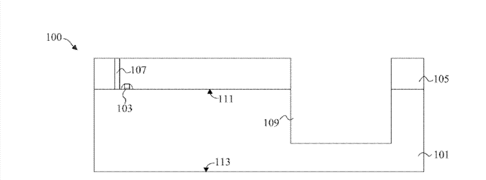
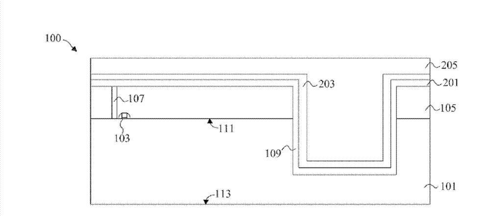
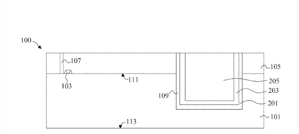
[0042] now refer to figure 1 , showing device 100 with substrate 101, active device 103 formed on substrate 101, first interlayer dielectric (ILD) 105 above substrate 101, passing through first ILD 105 to active device 103 Contacts 107 of the first ILD 105 and a first opening 109 formed through the first ILD 10...


PUM


Abstract

A system and method for forming through substrate vias is provided. An embodiment comprises forming an opening in a substrate and lining the opening with a first barrier layer. The opening is filled with a conductive material and a second barrier layer is formed in contact with the conductive material. The first barrier layer is formed with different materials and different methods of formation than the second barrier layer so that the materials and methods may be tuned to maximize their effectiveness within the device. The invention also provides an interconnect barrier structure and method.

Description

[0001] Cross References to Related Applications [0002] This application claims the benefit of US Provisional Patent Application Serial No. 61 / 503,991, entitled "Interconnection Barrier Structures and Methods," filed July 1, 2011, which is hereby incorporated by reference. technical field [0003] The present invention relates generally to the field of semiconductors and, more particularly, to interconnect barrier structures and methods. Background technique [0004] Typically, through substrate vias (TSVs) are formed in semiconductor wafers by pre-forming openings partially through the substrate. A barrier layer is formed to line the opening in order to prevent the diffusion of subsequently formed conductive material (e.g., copper) into the substrate, where this diffusion potentially degrades the overall performance of other devices formed on the semiconductor wafer. deteriorating. Likewise, the barrier layer also prevents damage caused by conductive materials. Once the...

Claims


Application Information

Patent Timeline
IPC IPC(8): H01L23/538H01L21/768
CPCH01L2224/05025H01L2224/03462H01L2224/05166H01L2224/05647H01L21/76847H01L2224/05186H01L24/03H01L2224/0345H01L24/05H01L2224/0401H01L21/76898H01L2224/05181H01L2224/05548H01L2224/05624H01L23/481H01L23/538H01L21/768H01L2924/15788H01L2924/00014H01L2924/04941H01L2924/04953H01L2924/00
Inventor 余振华邱文智吴仓聚
Owner TAIWAN SEMICON MFG CO LTD
Features
  • R&D
  • Intellectual Property
  • Life Sciences
  • Materials
  • Tech Scout
  • Unparalleled Data Quality
  • Higher Quality Content
  • 60% Fewer Hallucinations
Learn More