Semi-conductor conveying device

A conveying device and semiconductor technology, which is applied to conveyor control devices, conveyor objects, transportation and packaging, etc., can solve the problems of difficult adjustment, low work efficiency, and increased production costs, so as to avoid material waste and reduce production. Cost and work efficiency

Inactive Publication Date: 2013-01-09
JIANGYIN GLORY TECH
View PDF4 Cites 4 Cited by
  • Summary
  • Abstract
  • Description
  • Claims
  • Application Information

AI Technical Summary

Problems solved by technology

[0004] At present, the traditional transportation methods of semiconductors are as follows: figure 1 As shown, the semiconductor enters the conveying track 1 of the machine through the vibrating container, and the product blocking pin 2 at the front end of the conveying track 1 presses the semiconductor at the front end, and the rear motor drives the pick-up head 3 to move forward, and the pick-up head 3 is provided with a thimble trigger 4. Since the product blocking pin 2 has a wedge-shaped structure, the product blocking pin gradually releases the semiconductor product during the process of the pick-up head moving forward, and the semiconductor is blown to the pick-up head by compressed air. Due to the process of the pick-up head moving In the process, the product blocking needle has gradually loosened the semiconductor product. Before the pick-up head reaches the pick-up position, the compressed air may have blown the semiconductor out, so that the semiconductor product is not blown into the pick-up head, resulting in material drop. Occurs, resulting in waste of products, a corresponding decrease in production efficiency, and an increase in production costs
[0005] There is also a delivery method such as figure 2 As shown, the pick-up head is divided into two parts: the base plate 5 and the pick-up head 3. When working, the pick-up head is first moved to the pick-up position, and then the base plate is moved so that the thimble trigger gradually pushes away the product blocking pin. , and then the compressed air blows the front-end semiconductor product into the pick-up head, and then the bottom plate is retreated first, and the thimble trigger is gradually separated from the product blocking pin, so that the product blocking pin re-presses the front-end semiconductor, and finally the pick-up head is in the Return to the original position. This conveying method moves the pick-up head forward one step at a time, and compresses it one step at the time of exit, which can effectively avoid the phenomenon of material dropping. However, this method has many parts and complex structure. , and the steps are relatively cumbersome, once the process is confused, it is difficult to adjust, and the work efficiency is low

Method used


Image

  • Semi-conductor conveying device
  • Semi-conductor conveying device
  • Semi-conductor conveying device

Examples


Embodiment 1

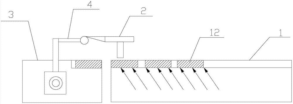
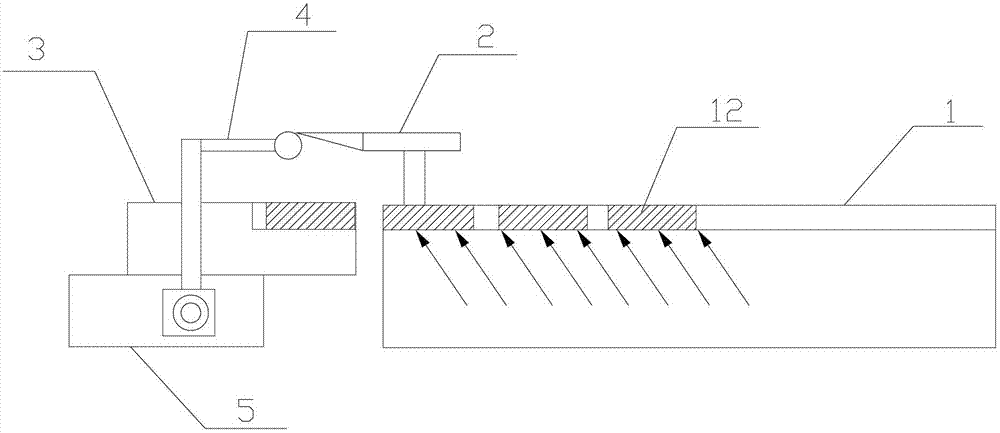
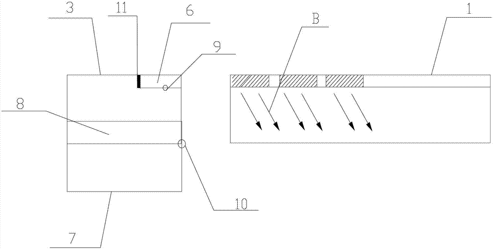
[0032] Please also see Figure 3 to Figure 5 , image 3 It is a structural schematic diagram of a semiconductor delivery device disclosed in the present invention. Figure 4 It is a structural schematic diagram of a semiconductor delivery device disclosed in the present invention when picking up semiconductors. Figure 5 It is a structural schematic diagram of a semiconductor conveying device disclosed in the present invention after picking up the semiconductor. As shown in the figure, a semiconductor conveying device is applied to a turntable test, printing and braiding machine. The conveying device includes a base 7, a conveying track 1, and a pick-up head 3 located at the output end of the conveying track 1 for receiving semiconductors. And a drive mechanism (not shown) that drives the pick-up head 3 to move back and forth on the base 7 . The driving mechanism can be a motor or an air cylinder, which drives the pick-up head to move back and forth to receive the semicondu...

Embodiment 2

[0040] The rest are the same as in Embodiment 1, except that a buffer mechanism is provided on the inner wall of the groove 6. Since the compressed air is to ensure that the semiconductor product is effectively blown into the groove, the conveying force may be relatively large, which may easily cause the semiconductor product to collide. Bad. By arranging the buffering mechanism, an effective buffering effect can be played when the semiconductor enters the groove, so as to avoid the impact damage of the semiconductor and reduce the cost.


PUM


Abstract

Disclosed is a semi-conductor conveying device. A switching mechanism is arranged to switch the release of compressed air in a conveying track and perform vacuum pumping operation. Before a pick-up head moves forward to a pick-up position, semi-conductors are absorbed on the conveying track mainly through vacuum and are prevented from falling off; and when the pick-up head moves to a pick-up position, the vacuum absorption force is canceled, the semi-conductors at the front end are blown to a groove of the pick-up head through the compressed air, then the semi-conductors at the back end are absorbed to the conveying track through switching the compressed air to the vacuum absorption, and the pick-up head moves to an original position simultaneously. According to the device, a product blocking needle and a center trigger of the existing device are omitted, parts are saved, falling off waste of the semi-conductors is avoided, the production cost is reduced, simultaneously, operation of the semi-conductors is achieved through the switching function between the compressed air and the vacuum absorption, and the working efficiency is high.

Description

technical field [0001] The invention belongs to the technical field of semiconductor packaging, and in particular relates to a semiconductor conveying device applied to a turntable test, printing and braiding machine. Background technique [0002] With the rapid economic development, my country has become one of the fastest growing semiconductor packaging markets in the world. However, the current level of domestic packaging is uneven, traditional packaging and advanced packaging coexist, and the overall level is relatively backward. In order to meet more challenges, it is necessary to improve the working performance of the test, printing and taping machine. At present, the rotary test printing and tape The all-in-one machine is widely used in the industry due to its advantages of high work efficiency and detection accuracy. [0003] The turntable test, printing and taping all-in-one machine is to place the bulk semiconductor transistors in the vibrating container and arran...

Claims


Application Information

Patent Timeline
Patent Type & Authority Applications(China)
IPC IPC(8): B65G47/88B65G43/08
Inventor 张巍巍
Owner JIANGYIN GLORY TECH
Why Eureka
Try Eureka