Selective metal surface treatment process and apparatus for circuit board and resist used in the process

Inactive Publication Date: 2007-12-06
UNIMICRON TECH CORP
View PDF9 Cites 4 Cited by
  • Summary
  • Abstract
  • Description
  • Claims
  • Application Information

AI Technical Summary

Benefits of technology

[0011]Accordingly, at least one objective of the present invention is to provide a selective metal surface tre

Problems solved by technology

1. The process needs to form a photoresist layer 150 having global coverage and perform an exposure and development process to expose the areas (that is, the second contacts 124) that need a nickel-gold layer. However, the actual area of some of the contacts 120 (that is, the first contact 122) that needs to be covered is only a very small portion of the area of the printed circuit board 100

Method used


Image

  • Selective metal surface treatment process and apparatus for circuit board and resist used in the process
  • Selective metal surface treatment process and apparatus for circuit board and resist used in the process
  • Selective metal surface treatment process and apparatus for circuit board and resist used in the process

Examples


Embodiment Construction

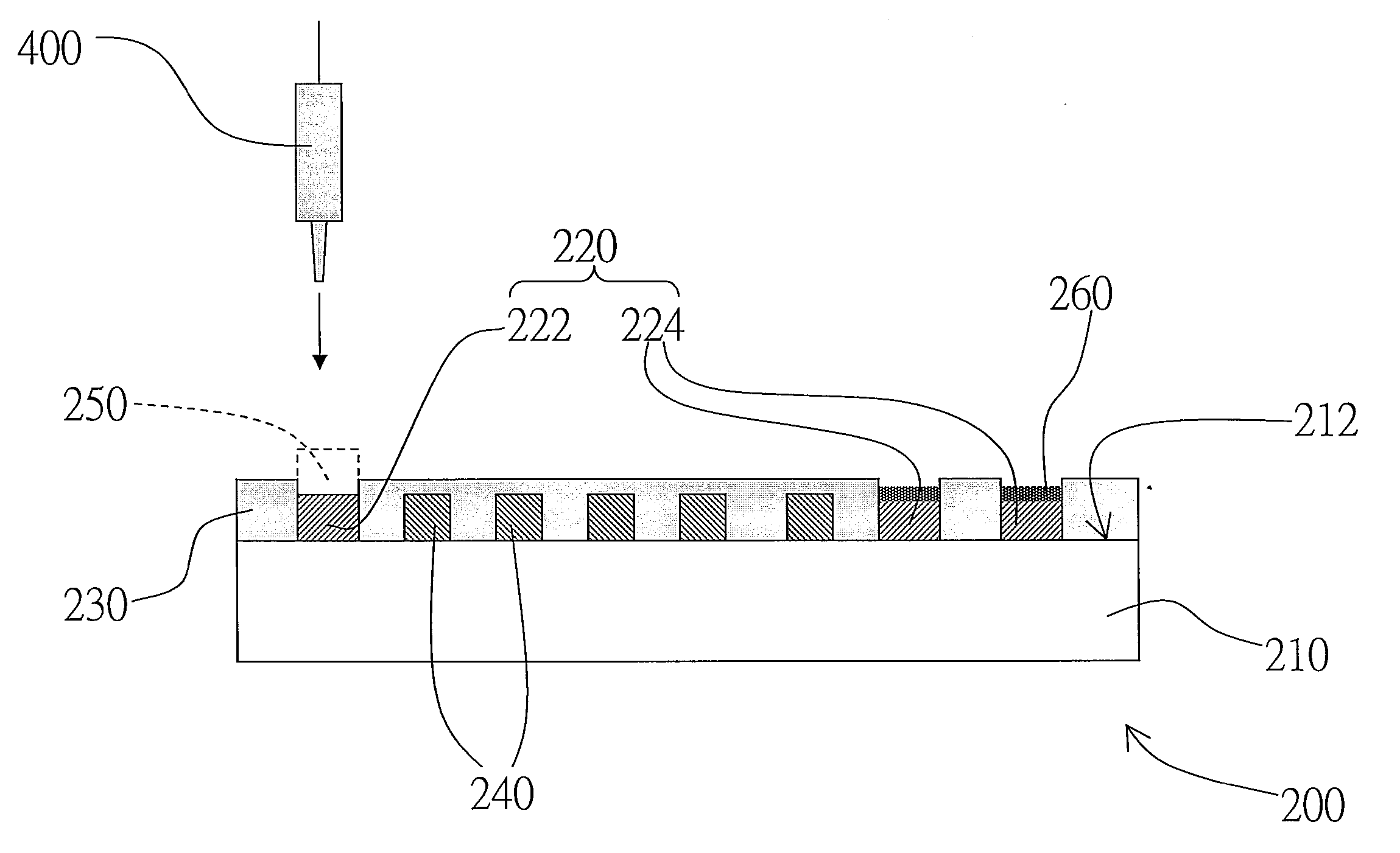
[0036]Reference will now be made in detail to the present preferred embodiments of the invention, examples of which are illustrated in the accompanying drawings. Wherever possible, the same reference numbers are used in the drawings and the description to refer to the same or like parts.

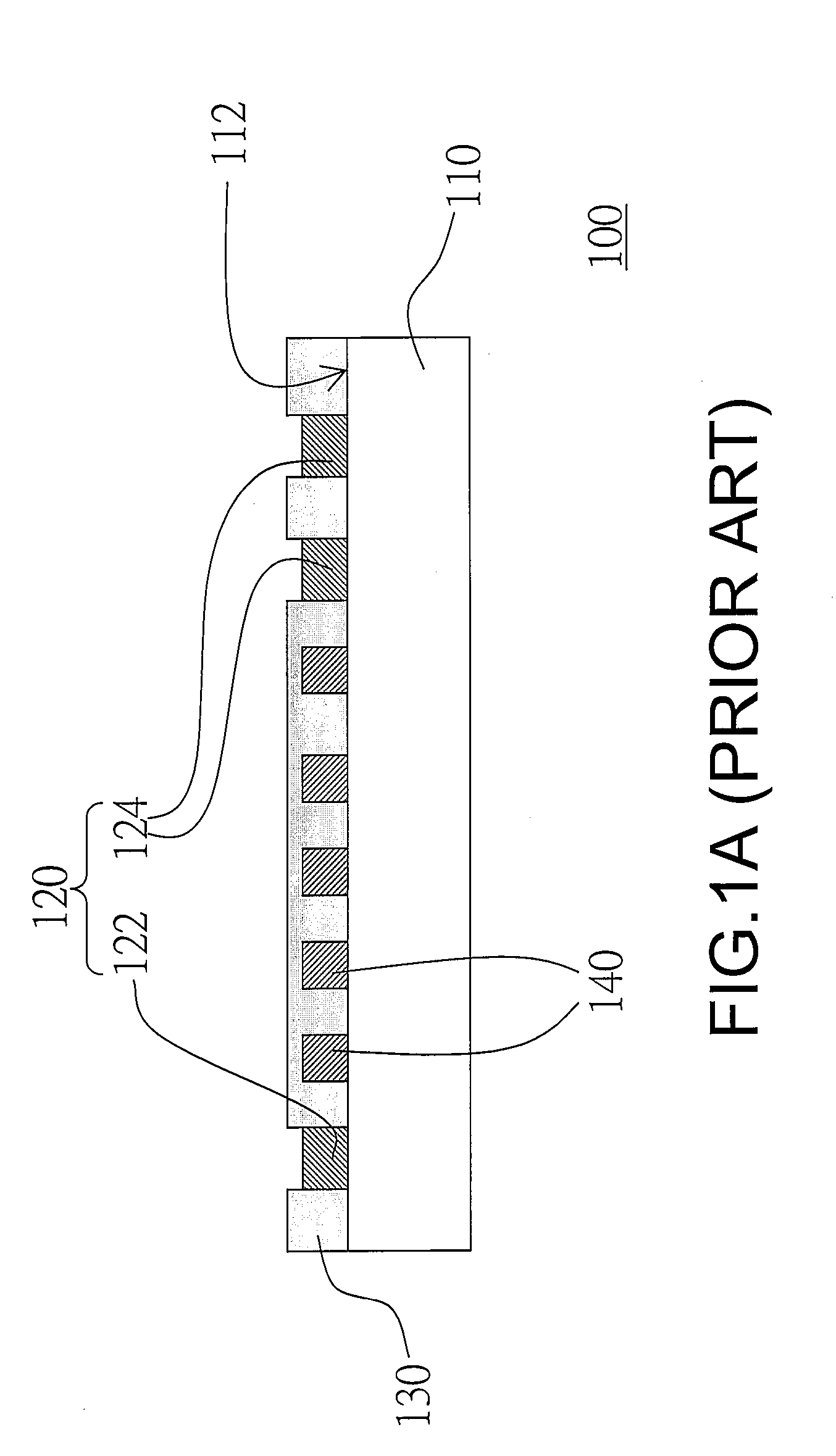
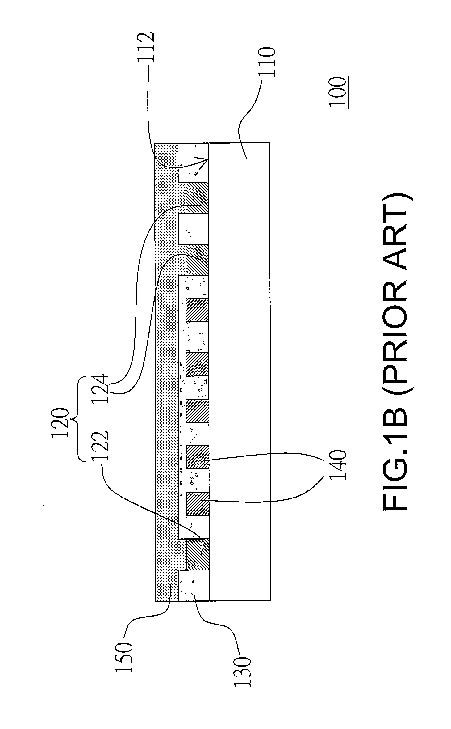
[0037]FIGS. 2A through 2D are diagrams showing the steps in a selective metal surface treatment process of a circuit board and its apparatus according to one embodiment of the present invention. As shown in FIG. 2A, the selective metal surface treatment process of a circuit board includes first providing a circuit board 200. The circuit board 200 has a substrate 210, a solder mask 230, a plurality of selective metal surface treatment areas 220 and a surface circuit 240. The substrate 210 may include a thin film, a multi-layered circuit board and / or a metal board, which serves as a carrier for the circuit board 200 and supports the surface circuit 240 and the selective metal surface treatment areas 22...


PUM


Abstract

A selective metal surface treatment process of a circuit board, which has a solder mask and a multiple of selective metal treatment surface areas, wherein the solder mask covers the surface of the circuit board but exposes the selective metal surface treatment areas, is provided. The selective metal surface treatment process includes using a printhead to selectively print a resist on a selective metal surface treatment area, performing a surface treatment of the other selective metal surface treatment areas, and removing the resist. A selective metal surface treatment apparatus used for performing the selective metal surface treatment process of the circuit board is also provided. Through the present invention, unnecessary waste of the materials in the process is reduced and the processing time is shortened.

Description

CROSS-REFERENCE TO RELATED APPLICATION[0001]This application claims the priority benefit of Taiwan application serial no. 95119341, filed Jun. 1, 2006. All disclosure of the Taiwan application is incorporated herein by reference.BACKGROUND OF THE INVENTION[0002]1. Field of the Invention[0003]The present invention relates to a circuit board process and related apparatus and material, and more particularly, to a selective metal surface treatment process, apparatus and material for a circuit board process.[0004]2. Description of Related Art[0005]With big advance in technologies and continuous improvement in the quality of life, together with the integration and sustained growth between the computer and communication industry, the fields of applications of integrated circuit (IC) is increasingly wide. Nowadays, integrated circuits are used in various electronic devices including, for example, notebook PC, cell phone, digital camera, personal digital assistant (PDA), printer and optical ...

Claims


Application Information

Patent Timeline
IPC IPC(8): H01L21/00H01L21/4763
CPCH01L21/6715H05K3/0076H05K3/0079H05K2203/058H05K3/28H05K2201/0391H05K2203/013H05K3/243
Inventor YU, CHENG-POYU, CHENG-HUNGCHANG, CHI-MIN
Owner UNIMICRON TECH CORP
Why Eureka
Try Eureka