Microscope device for detecting printed circuit board (PCB)

A microscope and microscopic imaging technology, which is applied in the direction of microscope, optical test defect/defect, optics, etc., to improve the detection effect and adaptability

Inactive Publication Date: 2013-01-09
SUZHOU SUNSHINE LASER & ELECTRONICS TECH CO LTD
View PDF6 Cites 7 Cited by
  • Summary
  • Abstract
  • Description
  • Claims
  • Application Information

AI Technical Summary

Problems solved by technology

[0003]However, the defect of the existing PCB microscope mentioned above is that it has poor adaptability to the size specifications of PCB products, and often can only meet the requirements of small size specifications (such as conventional 220mm× 160mm small-size PCB) PCB imaging inspection; and for PCBs with larger sizes (for example, the existing type of PCB can reach 650mm×710mm), it is often impossible to record the image of the entire PCB at one time. Of course, even by adjusting the

Method used


Image

  • Microscope device for detecting printed circuit board (PCB)
  • Microscope device for detecting printed circuit board (PCB)
  • Microscope device for detecting printed circuit board (PCB)

Examples


Embodiment

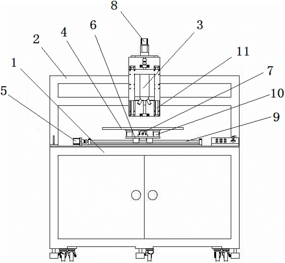
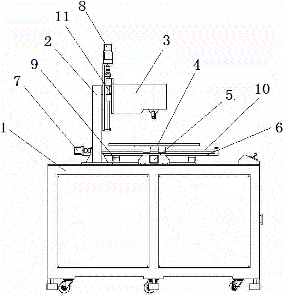
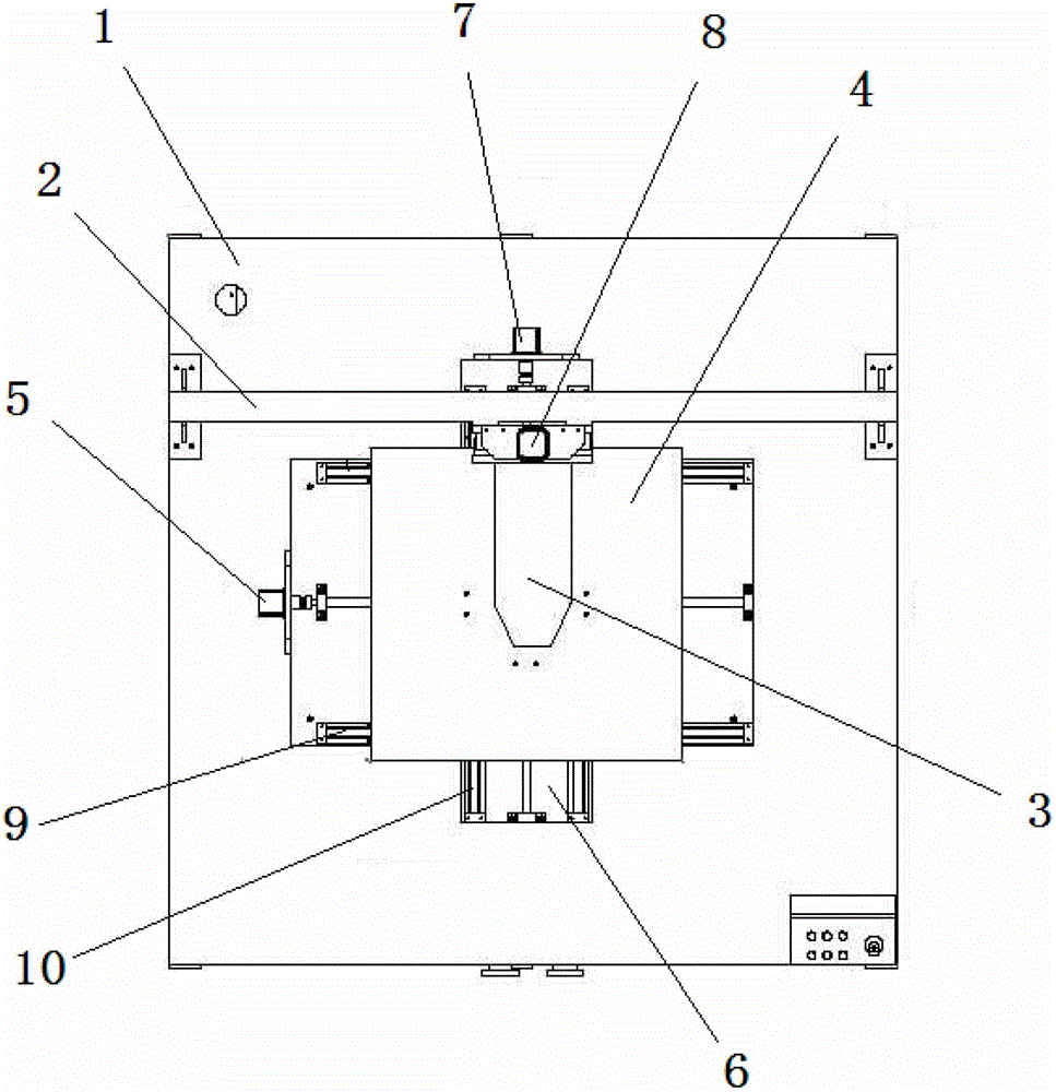
[0025] Example: Combined figure 1 , figure 2 and image 3 Shown is a specific implementation of the microscope device for PCB inspection provided by the present invention, which is mainly used for defect inspection of drilled PCBs. The microscope device for PCB detection consists of a working platform 1, a bracket 2, a CCD microscopic imaging lens 3, a PCB loading platform 4, an X-axis electric control screw transmission pair 5, a movable seat 6, a Y-axis electric control screw transmission pair 7, The Z-axis electronically controlled lead screw transmission pair 8, the X-axis linear guide rail 9, the Y-axis linear guide rail 10 and the Z-axis linear guide rail 11 are jointly composed.

[0026] A bracket 2 is fixed on the working platform 1, and the CCD microscopic imaging lens 3 is installed on the bracket 2 by means of a Z-axis electronically controlled screw drive pair 8, while the working platform 1 is equipped with an X-axis electronically controlled screw The ...


PUM


Abstract

The invention discloses a microscope device for detecting a printed circuit board (PCB), which comprises a working platform, a support which is fixed on the working platform, a charge coupled device (CCD) microscopic imaging lens which is installed on the support and a PCB carrying platform which is arranged below the CCD microscopic imaging lens; and the microscope device is characterized in that the working platform is provided with a movable seat through an X-axis electric-control lead screw transmission pair, the movable seat is provided with the PCB carrying platform through a Y-axis electric-control lead screw transmission pair, the CCD microscopic imaging lens is installed on the support through a Z-axis electric-control lead screw transmission pair, the Z axis is vertical to the working platform, and the X axis, the Y axis and the Z axis form a spatial right-angled coordinate system. The microscope device has high adaptability aiming at the PCB size specification and is convenient for the CCD microscopic imaging lens to carry out the fixed-point imaging photography on a detect part on the PCB, so that the detection effect is guaranteed.

Description

technical field [0001] The invention relates to a microscope device for PCB detection. Background technique [0002] With the development of electron microscope imaging technology, a special PCB microscope is usually used for defect detection on processed (for example, drilled) PCBs. Existing PCB microscopes mainly include two parts, one is a CCD microscopic imaging lens installed on a bracket and can be adjusted in height up and down, and the other is a PCB loading platform located below the CCD microscopic imaging lens. In actual work, by adjusting the focal length, the CCD microscopic imaging lens can record the complete imaging of the PCB below on a picture, and then the defect parts (breakage or spots, etc.) on the PCB are screened by computer or manually. [0003] However, the defect of the above-mentioned existing PCB microscope is that it has poor adaptability to the size specifications of PCB products, and often can only meet the imaging inspection of PCBs with sma...

Claims


Application Information

Patent Timeline
IPC IPC(8): G01N21/88G02B21/36
Inventor 沈祺舜
Owner SUZHOU SUNSHINE LASER & ELECTRONICS TECH CO LTD
Why Eureka
Try Eureka