Capacitive touch sensor, manufacturing method thereof, touch screen and display device

A touch sensor, capacitive technology, applied in the field of touch screen and display device, capacitive touch sensor and its manufacturing process, can solve the problem of high manufacturing cost of capacitive touch sensor, and achieve the effect of reducing manufacturing cost and reducing the number of use

Inactive Publication Date: 2013-01-09
BEIJING BOE OPTOELECTRONCIS TECH CO LTD
View PDF4 Cites 21 Cited by
  • Summary
  • Abstract
  • Description
  • Claims
  • Application Information

AI Technical Summary

Problems solved by technology

[0003] The purpose of the present invention is to provide a capacitive touch sensor and its manufacturing method, as well as a touch screen and a

Method used


Image

  • Capacitive touch sensor, manufacturing method thereof, touch screen and display device
  • Capacitive touch sensor, manufacturing method thereof, touch screen and display device
  • Capacitive touch sensor, manufacturing method thereof, touch screen and display device

Examples


Example Embodiment

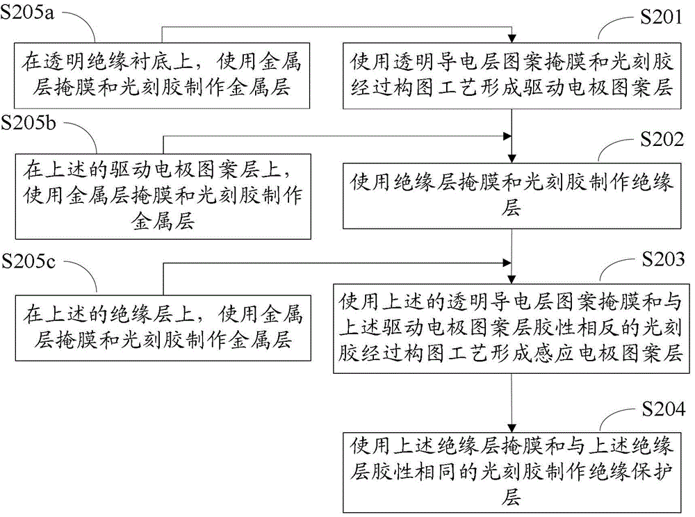
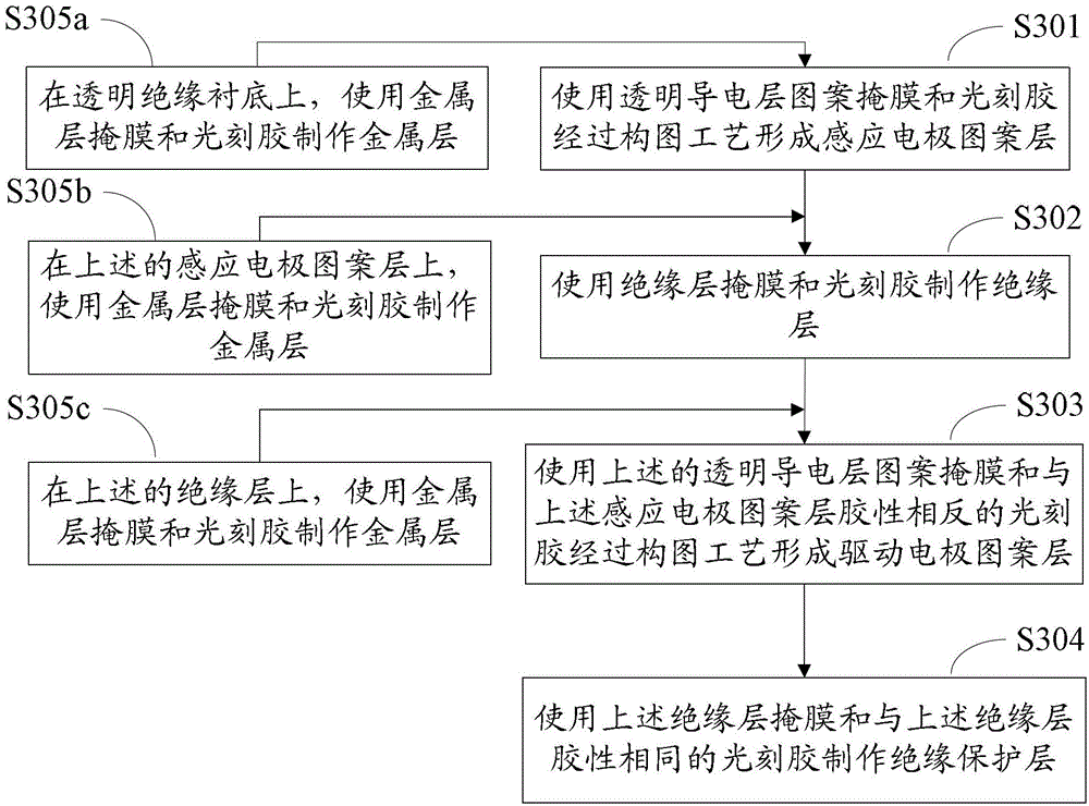
[0066] In order to reduce the manufacturing cost of the capacitive touch sensor, the embodiment of the present invention provides a manufacturing method of the capacitive touch sensor. figure 2 As shown, it specifically includes the following operations:

[0067] S201, using a transparent conductive layer pattern mask and photoresist to form a driving electrode pattern layer through a patterning process.

[0068] S202: Use an insulating layer mask and photoresist to make an insulating layer.

[0069] S203. Use the above-mentioned transparent conductive layer pattern mask and the photoresist with the opposite gel properties of the above-mentioned driving electrode pattern layer to form a sensing electrode pattern layer through a patterning process.

[0070] Wherein, the driving electrode pattern and the sensing electrode pattern form a complete transparent conductive layer pattern.

[0071] The aforementioned driving electrode pattern layer and the aforementioned sensing electrode patte...


PUM


Abstract

The invention discloses a manufacturing method of a capacitive touch sensor. The manufacturing method comprises the following steps of: manufacturing a drive electrode pattern layer by using a transparent conductive layer pattern mask and a photoresist; manufacturing an insulating layer by using an insulating layer mask and a photoresist; manufacturing a sensing electrode pattern layer by using the transparent conductive layer pattern mask and a photoresist which has the stickability opposite to that of the drive electrode pattern layer, wherein the drive electrode pattern layer and the sensing electrode pattern layer are located at different sides of a plane where the insulating layer is located; and manufacturing an insulating protection layer by using the insulating layer mask and a photoresist. The invention further discloses a capacitive touch sensor, a touch screen and a display device. As the insulating layer and the insulating protection layer are manufactured by using the same mask, the consumption number of masks is reduced, and then, the manufacturing cost of the touch screen is reduced. Furthermore, the sensing electrode pattern layer and the drive electrode pattern layer which are provided with transparent conductive layer patterns are respectively formed at different sides of the insulating layer, so that electric field lines from a drive electrode to a sensing electrode are enabled to be more divergent, and the sensitive touch degree is increased.

Description

technical field [0001] The present invention relates to the field of touch technology, in particular to a capacitive touch sensor and its manufacturing process, as well as a touch screen and a display device including the capacitive touch sensor. Background technique [0002] The capacitive touch panel (touch screen) has gradually developed into a mainstream touch screen due to its good performance and user experience. Capacitive Touch Sensor (touch sensor) is the key component of capacitive touch screen. The structure of the existing capacitive touch sensor usually includes: a transparent insulating substrate, the first layer made on the transparent insulating substrate is a metal layer, the second layer is an insulating layer, and the third layer is an ITO (nano indium tin metal oxide) pattern layer, and the fourth layer is an insulating protective layer. figure 1 Shown is a schematic diagram of a triangular ITO pattern layer, the pattern composed of multiple white trian...

Claims


Application Information

Patent Timeline
IPC IPC(8): G06F3/044
Inventor 刘英明王海生杨盛际
Owner BEIJING BOE OPTOELECTRONCIS TECH CO LTD
Why Eureka
Try Eureka