Thermal interface material and semiconductor packaging structure

A thermal interface material and packaging structure technology, applied in semiconductor devices, semiconductor/solid-state device parts, electric solid-state devices, etc., can solve the problems of reduced thermal conductivity, internal chip electrical short circuit, high cost of indium sheet materials, etc.

Inactive Publication Date: 2013-01-09
ADVANCED SEMICON ENG INC
View PDF8 Cites 33 Cited by
  • Summary
  • Abstract
  • Description
  • Claims
  • Application Information

AI Technical Summary

Problems solved by technology

However, during the high-temperature bonding process, the indium sheet will have fluidity due to the molten state, and the flow of the indium sheet means that it cannot be effectively bonded to the heat sink, and the heat conduction effect will be greatly reduced
In addition, the flowing indium flakes may also cause electrical short circuits in the internal chips of the semiconductor package
Furthermore, the material cost of indium sheet is relatively high

Method used


Image

  • Thermal interface material and semiconductor packaging structure
  • Thermal interface material and semiconductor packaging structure
  • Thermal interface material and semiconductor packaging structure

Examples


Embodiment Construction

[0014] In order to make the above-mentioned purposes, features and advantages of the present invention more obvious and understandable, the preferred embodiments of the present invention will be specifically cited below, together with the accompanying drawings, for a detailed description as follows:

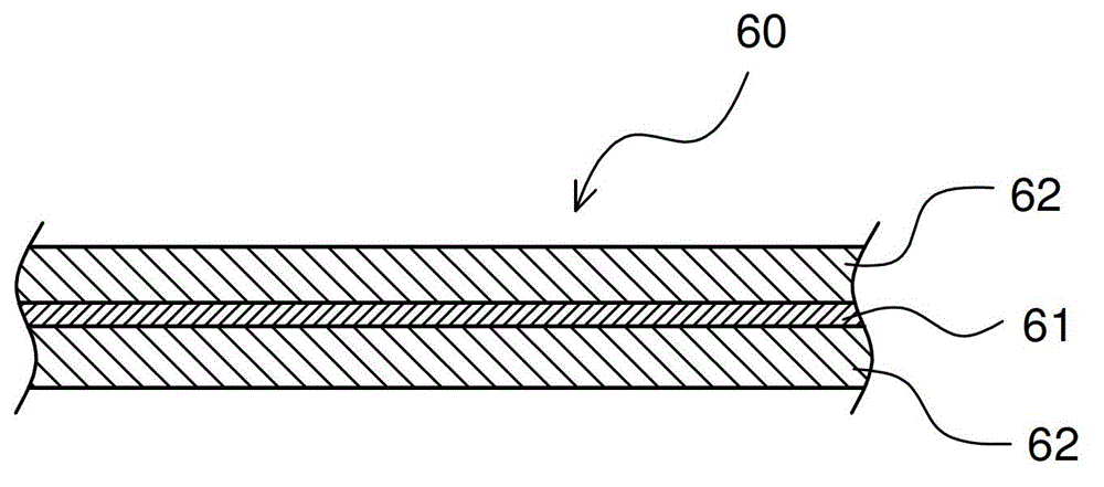
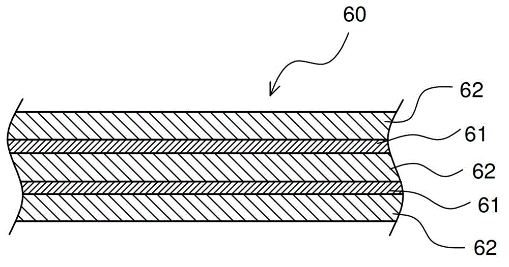
[0015] Please refer to figure 1 as shown, figure 1 is a side sectional view of a thermal interface material according to an embodiment of the present invention. The thermal interface material 60 includes a graphene layer 61 and two low-melting-point metal layers 62 , and the low-melting-point metal layer 62 covers the graphene layer 61 in a vertical arrangement.

[0016] Graphene is a two-dimensional material with a hexagonal honeycomb lattice composed of carbon atoms in sp2 hybridized orbitals and a thickness of only one carbon atom. It is worth noting that the thermal conductivity of graphene in the two-dimensional xy plane direction can be as high as 5300W / mK, but its therma...


PUM

PropertyMeasurementUnit
melting pointaaaaaaaaaa
thicknessaaaaaaaaaa
thicknessaaaaaaaaaa

Abstract

The invention discloses a thermal interface material and a semiconductor packaging structure. The semiconductor packaging structure comprises a substrate, a chip and a heat dissipation plate. The chip is arranged on the substrate, and the heat dissipation plate is arranged on the chip. The thermal interface material is contained between the chip and the heat dissipation plate; the thermal interface material comprises a grapheme layer and two low-melting-point metal layers; the two low-melting-point metal layers are covered on the grapheme layer from top to bottom. According to the thermal interface material and the semiconductor packaging structure, the flat heat-transfer efficiency between the chip and the heat dissipation plate can be improved through the grapheme material with high thermal conductivity; and the cost is lower than that of the thermal interface material using pure indium.

Description

technical field [0001] The invention relates to a thermal interface material and a semiconductor package structure, in particular to a thermal interface material composed of graphene and a low melting point metal and a semiconductor package structure with the thermal interface material. Background technique [0002] Existing high-end semiconductor chips (such as logic operation chips) or stacked semiconductor chips tend to generate high temperature during operation, so a heat sink needs to be bonded to the surface to improve the overall heat dissipation efficiency. The common method of fixing the heat sink on the chip is to use thermally conductive adhesive, but it is not easy to control the thickness uniformity of the thermally conductive adhesive when bonding, and the thermal conductivity of the contained metal thermally conductive particles is also worse than that of pure metal materials. [0003] In order to meet the high heat dissipation requirements of semiconductor pa...

Claims


Application Information

Patent Timeline
Patent Type & Authority Applications(China)
IPC IPC(8): H01L23/373B32B15/04
Inventor 李炳仁蔡宗岳高金利杨金凤
Owner ADVANCED SEMICON ENG INC
Why Eureka
Try Eureka